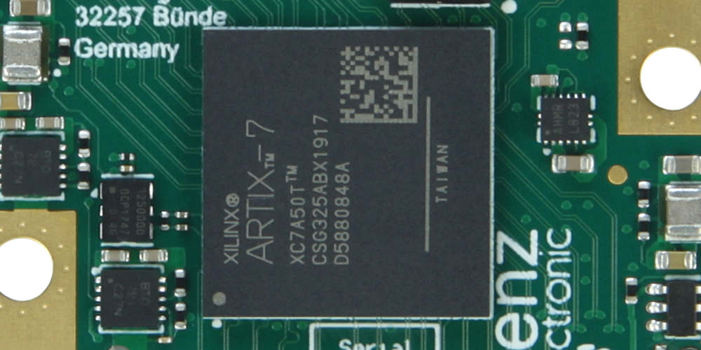
The Xilinx AC701 Evaluation kit includes the system performance for every watt Artix-7 family. This helps in getting you a quick prototyping to serve applications that are cost sensitive. This includes the components of IP, design tools, and reference designs that are pre-verified.
Also, this features a reference design that enables serial connectivity of high performance, as well as an advanced memory interfacing that is equipped with a complete license for the DMA engine.
What are the Main Features and Benefits of the Xilinx AC701?
- IP, design tools, hardware, and reference designs that are pre-verified
- Optimized for fast prototyping, and cost sensitive applications, making use of the Xilinx Artix-7 FPGAs
- Expand I/O using the FMC (FPGA Mezzanine Card) interface
- Implement the applications of visual display with the HDMI out
- Develop different networking applications with an Ethernet of 10-100-1000 Mbps.
- It supports the embedded processing using soft 32bit, MicroBlaze RISC
- Enables serial connectivity of high-performance with the GTP ports on SMA, SFP, and FMC
- References the design implemented with the engine of the Northwest Logic DMA, which is attached onto the AXI interface
- Demonstrates a data transfer system of high performance making use of a PCI Express
- Memory interface that is advanced with DDR3 SODIMM of 1GB and up to 1066Mbps/533MHz
SD Card Interface
The xilinx AC 701 board features a digital input/output interface that is secure. This is done in order to offer the user-logic access to the non-volatile general purpose SD10 peripherals and memory cards. Also, the slot for the SD card is mainly designed for supporting high-speed SD cards at 50MHz. The connection of the SD10 signal is done to the input/output block, and its VCCO is usually set to about 3.3V.
Quad SPI Flash Memory
This flash memory offers 250 mb of a non volatile storage, which is useful for data storage and configuration. It has a supply voltage of 3.3V and a data path width of 4 bits. Here, the data rate is different depending on the Quad/Dual/Single mode, as well as CCLK rate. The pin of the FPGA CCLK, as well as four data lines, is usually wired in the flash memory of the Quad SPI.
USB JTAG Module
The provision of the JTAG configuration is made possible via the onboard USB to JTAG configuration, where some computer accesses the JTAG chain of the xilinx AC701 board via the A plug (standard) to the micro-B plug USB cable. Furthermore, a JTAG header of 2mm is provided, as well in parallel for the download cables of xilinx to access like the parallel code IV as well as cable USB II.
System Clock Source
The Xilinx AC701 board features an LSDS differential oscillator of 2.5V and 200 MHz. These are soldered onto the board’s back side and also wired into the clock input of the FPGA MRCC.
Programmable User Clock
The xilinx AC701 board features a low-jitter programmable differential oscillator of 3.3V that drives the inputs of the FPGA MRCC. On power-up, this user clock enters into default in an output frequency that can reach 156.250 MHz. Also, via the I2C interface, the user applications will be able to alter the output frequency within the 10 MHz – 810 MHz.
GTP Transceiver Clock Multiplexer
The xilinx AC701 board offers flexible GTP Quad options by using external multiplexer components U4 and U3 to help in servicing the GTP Quad SMA, FMC, and SFP MGT interfaces. Each multiplexer features a clock source, which is present in about three of the four inputs. Note that the fourth input isn’t connected.
Jitter Attenuated Clock
The xilinx AC701 board features Silicon Labs jitter attenuator present on the board’s back side. Here, the FPGA user will be able to implement the clock recovery circuit. Also, it will be able to output the clock to a differential input/output pair on the input/output bank.
The main purpose of the clock is to offer support to the OBSAI/CPRI applications, which perform the clock recovery from the user-supplied SFP+/SFP module and then use this jitter attenuated clock for the driving of the GTP transceiver’s reference clock inputs.
What are the Board Features of the Xilinx AC701?

Clocking
- Attenuated jitter clock
- Differential GTP SMA clock input
- Differential SMA reference clock input
- Serve as a system clock for FPGA
- Fixed oscillator having a differential ouput of 200MHz
- User programmable differential oscillator that falls within the range of 10MHz to 810 MHz
- Serves as the FPGA’s system clock
Networking and Communication
- SFP cage
- UART to the USB bridge
- GTP port that features 4 SMA connectors
- Ethernet of 10, 100, or 1000 Mbps
- 4-lane PCI Express edge connector
Expansion Connectors
- PMOD (0.1” 1×6 Header)
- VADJ which can offer support 3.3V, 2.5V (which is the default), or 1.8V
- FMC-HPC connectors that are partially populated
- 2 GTP transceivers, 58 differential or 116 single ended user defined signals
Configuration
- SPI flash (quad) of 32mb
- JTAG header offered to be used with the download cables of Xilinx like the cable USB II
- Circuitry of the JTAG configuration to ensure configuration over the USB
I/O and Control
- SMA user input/output (diff pair)
- DIP switch of the user
- Push buttons of the user (x5)
- 7 input/output pins available via LCD header
- FAN header (AMS)
Memory
- It has a slot for the memory card
- The IIC EEPROM with a size of 8kb
- Quad SPI slash is 32mb
- DDR3, SODIMM of 1 Gb and can reach 523MHz and 1066 Mbps
Power
- AC power adapter of 12V
- Display
- 4 user LEDs
- 2 x 16 LCD display
- HDMI output for video
Conclusion
Here comes the end of our article on the xilinx AC701 evaluation kit. This kit comes with great features and it includes the system performance for every watt Artix-7 family. This helps in getting you a quick prototyping to serve applications that are cost sensitive.