Logic circuit development is a continuous process that changes drastically with time. Getting the best Field Programmable Gate Arrays (FPGAs) is therefore important to provide you with the best logic circuit designing solutions. We can achieve this using high-end FPGAs, which aid in accelerating critical network functions. However, FPGAs are evolving, and designers are working on making better FPGAs that will be more compatible with many computers. Current FPGAs are easier to program since they support AXI (Advanced Extensible Interface) buses. We often need to connect our FPGAs to the CPU using the available connection ports to boost the computers’ speed. However, not all FPGA boards support these connections, hindering the development of AI (Artificial Intelligence). Therefore, we should consider the most reliable FPGAs in our logic circuit designing processes. The following are the top 12 high-end FPGA chips.
Terasic De10Nano Kit
The De10Nano is a low-cost single-board computer that contains the Cyclone V SoC. In addition, the board has an HDMI port, an Ethernet port, a USB port, and numerous other peripherals. Furthermore, DE10-Nano is compatible with computer vision, image processing, audio processing, and further applications. Equally important is that the Cyclone V SoC on the DE10Nano has a dual-core ARM Cortex-A9 processor, FPGA fabric, and many peripherals. Additionally, the FPGA fabric is appropriate for time-sensitive, high-performance applications, including image, video, and audio processing. Finally, we can power the DE10Nano using any 5V supply or a USB OTG port.
Moreover, the DE10Nano is a fantastic choice for numerous applications, such as computer vision, image processing, audio processing, and more. Additionally, the board is a great place to test new ideas and build prototypes since it is affordable and has a lot of functions. In addition, Terasic DE10Nano is a cyclone-based SoC FPGA that provides IoT system developers, educators, and makers with a platform for programmable hardware creation. The board also has high-speed DDR3 memory, a double CPIO extension connection, and improved analog-to-digital conversion capabilities.
Features
The DE10Nano features an HDMI port, a USB OTG connector, an Ethernet port, and several extra peripherals and extension adapters. Moreover, the board also contains a microSD card slot for storage.
Spartan 6
Spartan 6 FPGA is a member of the Xilinx generation. In addition, manufacturers of the Spartan 6 family’s products apply Xilinx’s 65nm silicon-on-insulator (SOI) method during fabrication. Moreover, the board contains features like embedded block RAM, DSP slices, and high-speed serial transceivers. Equally important is that the Spartan 6 family offers power-gating and power-saving techniques. Furthermore, the Spartan 6 series is applicable in numerous fields due to its high level of integration and adaptability. For instance, storage, video processing, and fast networking are all possible uses for the Spartan 6. Additionally available is the Spartan 6 LX, a low-cost Spartan 6 derivative targeted for high-volume applications. Moreover, Xilinx has numerous development tools to support the Spartan 6 family, including the ISE Design Suite.
Features
The following are some of the Spartan 6 FPGAs’ key features:
- Low-power operation
- High-speed serial transceivers
- On-chip memory
- Fast wake-up response time
- DSP48A1 slices
Basys 3

The Basys 3 is one of several field-programmable gate arrays (FPGAs) designed with novice users in mind. Basys 3 provides embedded systems designers with a cost-effective environment for prototyping digital circuits. Furthermore, it is fully compatible with the widely used Vivado Design Suite. Designers have made the Basys 3 board the newest member of the famous Basys family of FPGA development boards, with Vivado IP Integrator compatibility in mind.
In addition, the board includes a Spartan-6 LX9 FPGA from Xilinx, along with 4 MB of SPI Flash memory, 128 MB of DDR2 SDRAM, USB-JTAG programming circuits, a USB UART, clock sources, switches, LEDs, buttons, and other customary features. Equally important is that each of the fast DSP48A1 slices of the Xilinx Spartan-6 FPGA can do one multiple-accumulate operation of 24 bits by 18 bits per clock cycle. The Spartan-6 FPGA also supports a broad range of I/O operations and supports Gigabit Ethernet, USB 2.0, and LVDS. The Basys 3 board, which comes with a wide range of free IP, tools, and tutorials, is a fantastic platform for learning about FPGAs.
Features
The Spartan-6 FPGA board has a wide range of features such as:
- 50K logic cells
- Onboard USB
- Xilinx Artix-7 FPGA
- UART bridge
- 4-bit LED display
- MicroSD card slot
- JTAG programming circuitry
- Temperature sensor
- Power supply LED
- Two user switches (SW1, SW0)
- External clock support
- 100MHz clock speed
- Reset button
- 4 Pmod ports
- Quad-SPI Flash (256Mb)
- External power supply support (3.3V)
- Onboard power-on LED etc.
Zybo Z7
Zybo Z7 is a ready-to-use digital circuit and software development board of the Xilinx Zynq-7000 family, with various improved features. In addition, the Zynq family operates based on AP SoC Xilinx programmable on-chip system architecture. Furthermore, the chip integrates the Xilinx 7-series FPGA (Field Programmable Gate Array) logic with a dual-core ARM Cortex-A9 processor.
Additionally, the Zybo Z7 offers a rich set of connectivity and multimedia peripherals to the Zynq, creating a formidable mono-board computer before considering the power and flexibility added by the Field Programmable Gate Array (FPGA). Equally important is that the Zybo Z7 has a video-capability feature with an HDMI input, a MIPI CSI-2 compatible Pcam connector, high DDR3L bandwidth, and an HDMI output. These features, therefore, allow for high-end embedded vision capabilities that make Xilinx FPGAs famous. Moreover, the Zybo Z7 has Pmod connectors that enable you to attach additional hardware such as Pmod peripheral boards, allowing access to such devices as sensors, motor controllers, displays, etc.
Features
Zybo Z7 has the following features:
- Memory
The chip has a 1 GB memory with a 1066 MHz DDR3L 32-bit bus. Additionally, the board has a MicroSD slot and a 16 MB Quad-SPI 128-bit flash compatible with the 48-bit global EUI-48/64 identifier.
- Audio and video
Zybo Z7 has an HDMI sink port (input) and an HDMI source output port with CEC. Additionally, it has an audio codec with a stereo line-in, microphone jacks, and stereo headphones. Furthermore, Zybo Z7 has a Pcam camera connector that is MIPI CSI-2 supported.
- Power
You can power the board from a USB or any 5V external power source.
- Ethernet and USB
The chipboard has a USB 2.0 OTG PHY port with device support and a host. In addition, the chip has a USB-UART bridge, USB-JTAG programming circuitry, and a Gigabit Ethernet PHY.
- Processor
The Zybo Z7 chipboard has a ZYNQ processor with the following features:
- USB 2.0, 1G ethernet, and SDIO high-bandwidth peripheral controllers
- An Artix-7 FPGA – equivalent programmable logic
- SPI, CAN, 12C, and UART low-bandwidth peripheral controllers
- 4 High-Performance AXI3 Slave ports and an 8 DMA-channelled DDR3L memory controller.
- Dual-core (667 MHz) Cortex-A9 processor
Nexys A7

Nexys A7 is a complete digital circuit development platform of the Xilinx family. Additionally, the board operates with the latest and up-to-date Artix-7 FPGA (Field Programmable Gate Array). Furthermore, this board has a large, high-capacity FPGA, a collection of ethernet and USB ports, and a tremendous external memory. The board can therefore host a variety of designs, from introductory combinational circuits to more complex embedded processors. In addition, the board has numerous in-built peripherals such as the temperature sensor, speaker amplifier, MEMs digital microphone, an accelerometer, and several input-output devices. These peripherals enable the board to perform various designs independent of other components.
Features
The Nexys A7 board has the following features:
- Memory
The board has a 128 MiB DDR2 memory, a microSD card slot, and a serial flash memory.
- USB and Ethernet
The board also has a USB-UART bridge, a USB-JTAG programming circuitry, a 10/100 Ethernet PHY, a USB HID mouse, keyboards, and a memory stick host.
- Power
You can power the board from any 4.5-5.5V external power source or a USB source.
- Audio and Video
The board has a PDM microphone, a PWM audio output, and a 12-bit VGA output.
- Expansion connectors
- Nexys A7 has four Pmod connectors that offer 32 FPGA input-output features and a XADC signal Pmod connector.
- Additional sensors
The board has a temperature sensor and a 3-axis accelerometer.
However, the Diligent Adept Utility does not support Nexys A7.
Pynq-Z1
Pynq Z1 is a sophisticated FPGA tool that allows developers to construct unique hardware designs quickly and efficiently. Additionally, Pynq Z1 operates based on the well-known Xilinx Zynq-7000 All-Programmable System-on-Chip (APSoC). Pynq Z1 also provides an all-inclusive development environment with everything required to create, debug, and deploy bespoke hardware designs. The integration of Pynq into existing development environments is simple. Furthermore, it delivers a comprehensive hardware development kit with a powerful Vivado IP Integrator and a complete software development kit with a comprehensive board support package. Additionally, a growing ecosystem of third-party hardware and software suppliers supports Pynq. Moreover, the third-party hardware and software ecosystem contains many resources that help speed up the creation of unique hardware designs.
Features
Memory
The board has a MicroSD slot, a 512 MB DDR3 with a 1050 Mbps 16-bit bus, and a 16MB Quad-SPI Flash compatible with the global 48-bit unique EUI-48/64.
Power
The board’s power can be from any 7V-15V source or a USB supply.
Audio and Video
Pynq-Z1 has an HDMI sink (input port), a PDM-interfaced microphone, an HDMI source (output port), and a PWM driven 3.5 mm jack mono audio output.
USB and Ethernet
The board has a USB-UART bridge, a Gigabit Ethernet PHY, a USB-JTAG programming circuitry, and a USB OTG PHY host port.
Switches, LEDs, and Push-buttons.
Pynq-Z1 has 4 LEDs, two slide switches, four push buttons, and 2 RGB LEDs.
Kintex 7
The Kintex 7 chip is a member of the Xilinx FPGAs based on a 28nm architecture. In addition, the design consumes low power, 50% below the earlier FPGAs’ power consumption rates. However, the cost performance has increased to about two times the initial cost. Xilinx Kintex 7 FPGAs offer memories, high-density logic, high-performance transceivers, DSPs, and mixed flexible signals. Therefore, you can improve the system-level performance and achieve better integration.
Moreover, the board has an on/off power supply sequencing and a working AC and DC switching capability. Furthermore, Kilintex 7 FPGAs have highly-integrated connectivity and a relatively higher speed. Equally important is that the board supports several air interfaces such as WiMax, LTE, and WCDMA.
Features
Kintex 7 Xilinx FPGAs have the following features:
- The density of Xilinx Kintex 7 FPGAs attains two million-logic units, which is about 2.5 times that of earlier FPGAs.
- The board also has a 10.3125 Gbps serial connection function.
- Kilintex 7 has an excellent block memory and abundant DSP resources.
- The board also has a 36 kb dual-port in-built block RAM FIFO logic that ensures on-chip data buffering.
- Xilinx also has a 3.3V VCCO HR I/O voltage bank.
- In addition, the board’s 72-bit memory interface supports a single memory buffer design as opposed to the typical two and four buffer methods.
Moreover, its memory controller has a complex and dedicated IP memory that enhances easier interfacing with the external DDR memory.
Nexys 4 DDR
Based on the Xilinx Spartan-6 FPGA, the Nexys 4 DDR is an entire, ready-to-use digital circuit creation platform. It is the most recent board in the well-known Nexys series of FPGA development boards and has the potent Spartan-6 device family. Compared to the Spartan-3 FPGA of the previous generation, the Spartan-6 FPGA delivers more than 50% more logic density and up to double the clock speed. It is well-suited for high-performance logic. Furthermore, the Nexys 4 DDR board includes a DDR SDRAM memory chip, USB programming, JTAG debugging circuitry, four PMOD connectors, an Arduino header, and other practical peripherals. Moreover, the board’s big-capacity FPGA offers enough logic resources for high-density applications. In addition, the Nexys 4 DDR is an excellent platform for learning and expert circuit design since it has a large variety of free and paid software tools.
Features
The Nexys 4 DDR board has the following features:
- 512kB Flash Memory
- User LEDs
- Xilinx Spartan-6 XC6SLX16-FGG484C FPGA
- Dual-role USB-UART/JTAG FTDI FT2232H chip
- PMOD and Arduino headers
- 4MB SRAM
- Micro SD Socket
- Temperature Sensor
- Arduino Host
- FTDI FT2232H USB-JTAG/USB-UART Bridge
- Analog devices AD5206 6-channel Digital Potentiometer
- Pmod Host
- External 2W Stereo Speaker
- 4-Digit 7-Segment display
- Analog Devices AD5228 2-channel Digital Potentiometer
- Analog Devices ADT7420 Temperature Sensor etc.
Zynq 7020
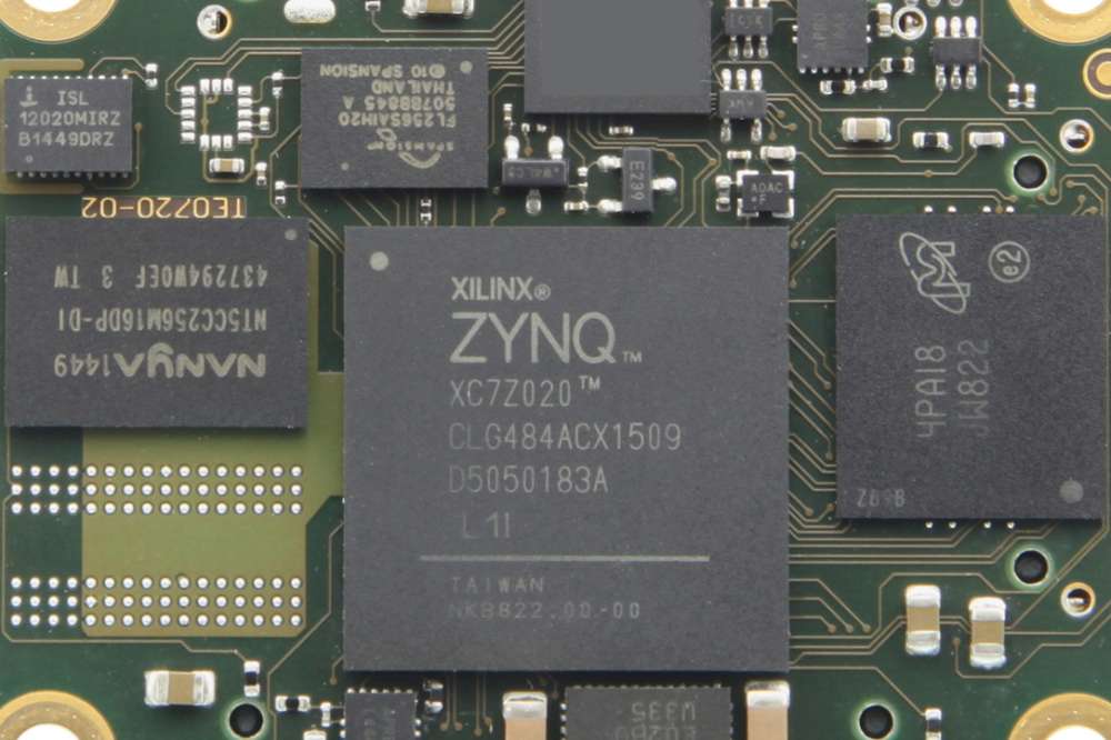
The Xilinx All Programmable SoC architecture is the foundation for the Zynq-7020 family. It combines the logic of a Xilinx 7-series Field Programmable Gate Array (FPGA) and a complete dual-core Arm Cortex-A9 processing system (PS) into a single unit. The PS’s components include a NEON coprocessor, a shared L1 cache, a PL310 L2 Cache Controller, a DDR3 Memory Controller, and an I/O subsystem. Moreover, it consists of the 28K logic cells, DSP slices, Block RAM, and I/O blocks that make up the Xilinx 7-series FPGA logic (PL). Moreover, the Zynq-7020 family combines a dual-core ARM Cortex-A9 MPCore processing system with an FPGA’s flexibility and scalability. In addition, it is a perfect choice for applications that need a mix of hardware and software programmability. For example, we can use the FPGA fabric to configure various I/O and memory interfaces available in the Zynq-7020 family.
Additionally, the Zynq-7020 family features a wide range of on-chip peripherals that we can customize using the FPGA fabric. A comprehensive set of development tools, including Vivado Design Suite, SDK, and IPI, is available to support the Zynq-7020 family. Moreover, the complete FPGA development environment known as the Vivado Design Suite includes logic synthesis, place and route, and bitstream creation. Furthermore, the SDK is an all-inclusive environment for developing software that comes with a C/C++ compiler, debugger, and profiler. Finally, the IPI is a collection of libraries and drivers that make creating unique IPs easier.
Features
Zynq 7020 has the following features:
- 7000 AP SoC
- Integrated Artix-7 FPGA logic
- Xilinx Zynq
- 512KB L2 Cache
- 32MB Quad-SPI Flash
- Gigabit Ethernet
- HDMI
- 4MB SRAM
- USB 2.0 Host
- USB 2.0 OTG
- UART
- 256MB DDR3 SDRAM (64 bit wide)
- 32KB D-Cache and 32KB I-Cache per processor
- 667MHz dual-core Cortex-A9 MPCore processor etc.
Nexys 4
Nexys 4 is an FPGA development board for teaching digital logic and hardware programming. In addition, the board includes a USB 2.0 interface, 64 MBit SDRAM, Xilinx Spartan-6 FPGA, and other peripherals. The Nexys 4 is, therefore, ideal for applications such as logic design, embedded systems, image processing, and signal processing, among others. Equally important is that we can utilize the Nexys 4 development board for thorough teaching in digital logic and programming hardware. The board has Xilinx Spartan-6 FPGA, a very effective tool for designing and implementing logic. In addition, the board contains a USB 2.0 connector, 64 Mbit SDRAM, and other accessories. Spartan-6 FPGA also consists of an effective on-chip processor that is useable for several tasks. In addition, the Nexys 4 development board has a USB 2.0 connector for both FPGA programming and external device communication.
Additionally, the board consists of a JTAG port for programming or debugging the FPGA. Moreover, the Nexys 4 development board is suitable for comprehensive digital logic and hardware instruction. Equally important is that the board has Xilinx Spartan-6 FPGA, a potent tool for designing and implementing logic. Additionally, the board consists of a 64 Mbit SDRAM, a USB 2.0 port, and other accessory interfaces. The Nexys 4 is also suitable for image processing, embedded systems, signal processing, etc.
Features
The Nexys 4 board has the following features:
- SD card slot
- VGA display
- USB port
- 7-segment display
- Audio output etc.
Max 10 Altera
Max 10 Altera is a member of the Intel Field Programmable Gate Array (FPGA) family. In addition, Max 10 Altera redefines a non-volatile integration by offering high processing capabilities in a cheap, tiny, single-chip programmable logic device. Furthermore, as an improvement from the prior Max devices’ single-chip history, Max 10 Altera offers a wide density range of between 2,000 and 50,000 LEs, using either dual or single-core voltage.
Additionally, the MAX 10 line of FPGAs has both advanced tiny wafer scale packaging (3 mm × 3 mm) and high I/O pin count packages. Moreover, the TSMC’s 55 nm embedded NOR flash technology enables instant-on capability in MAX 10 FPGAs. Integrated features like dual configuration flash & analog-to-digital converters (ADCs) also allow dynamic switching between two pictures stored on a single chip. Equally important is that MAX 10 FPGAs have full-featured FPGA capabilities, including Nios II soft core embedded CPU support, digital signal processing (DSP) blocks, and soft DDR3 memory controllers, in contrast to CPLDs.
Features
Max 10 Altera has the following features:
- Dual-port RAM
- Flash memory
- PLL
- Supports boundary-scan and JTAG scan testing
- Compatible with all Altera FPGA generations
- Wide range of input/output capabilities
Spartan 3e
Spartan-3E is a family of Xilinx field programmable gate array (FPGA) devices. In addition, it distinguishes itself with a fair price and small size. Furthermore, the Spartan-3E family’s FPGAs were the first ones on the market to have system-level integration features like built-in multipliers, block RAM, and sophisticated power management. Therefore, spartan-3E FPGAs are ideal for high-volume, budget-conscious applications like industrial control, security, and consumer electronics. Moreover, The Spartan-3E family includes products with different densities, package sizes, and I/O capabilities. Spartan-3E FPGAs are available in densities starting at 1.5 million system gates and the 6-input LUT4 architecture from Xilinx.
Equally important is that the smallest container that Spartan-3E FPGAs are now available in the new ChipScale Packaging (CSP) from Xilinx, with a footprint of just 3 mm x 3 mm. Spartan-3E FPGAs also have the highest I/O pin-count density currently available, with up to 1,280 I/O pins in a single package. In addition, Spartan-3E FPGAs are the first FPGAs available on the market that provide sophisticated power management features, including Select I/OTM power reduction and PowerPlayTM early power estimation. Furthermore, with devices requiring as little as 50 mW at 1.2V, Spartan-3E FPGAs also offer the lowest static power consumption.
Features
The following are the features of the Spartan-3E FPGS boards:
- Flip-flops
- In-system programmability
- 2.5V and 3.3V power options
- Single-ended and differential I/O
- Selectable I/O standards
- Spartan 3E field-programmable gate array
- Four input look-up tables (LUTs)
- Fast configuration download
- JTAG boundary-scan
- Fast, low-cost FPGA
- 110,000 logic cells (LCs)
- Wide range of I/O capabilities
- Global and regional clocking resources
Conclusion
The above information highlights the top 12 high-end Field Programmable Gate Arrays. Controlling these FPGAs’ chips requires us to have an emulation circuit that may run slower than the actual circuit. The process of designing logic devices will therefore be accurate and easier to follow. Additionally, such applications as the Internet of Things (IoT), sensor controlling, and display platforms will be easier to achieve. However, we look forward to better chips with a limited focus as opposed to the current general-purpose chips. Consequently, the electronic world will become a programmable System-on-a-chip (SoC).