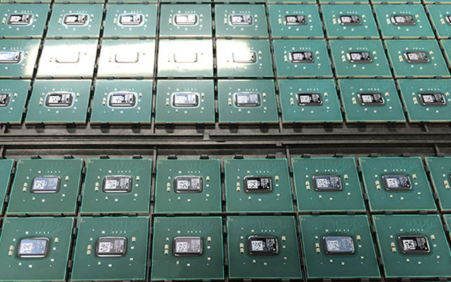
XC2018TM-33PC84I ApplicationField
-Cloud Computing
-Internet of Things
-Consumer Electronics
-Artificial Intelligence
-Wireless Technology
-Industrial Control
-5G Technology
-Medical Equipment
Request XC2018TM-33PC84I FPGA Quote , Contact Sales@ebics.net Now
XC2018TM-33PC84I FAQ

Q: Where can I purchase Xilinx XC2018 Development Boards, Evaluation Boards, or XC2000 Logic Cell Array Starter Kit? also provide technical information?
A: EBICS does not provide development board purchase services for the time being, but customers often consult about ZedBoard, Basys 3 board, TinyFPGA BX, Nexys4-DDR, Terasic DE10-Nano, Digilent Arty S7, etc. If you need relevant technical information, you can submit feedback information, our technicians will contact you soon.
Q: Do I have to sign up on the website to make an inquiry for XC2018TM-33PC84I?
A: No, only submit the quantity, email address and other contact information required for the inquiry of XC2018TM-33PC84I, but you need to sign up for the post comments and resource downloads.
Q: Does the price of XC2018TM-33PC84I devices fluctuate frequently?
A: The EBICS search engine monitors the XC2018TM-33PC84I inventory quantity and price of global electronic component suppliers in real time, and regularly records historical price data. You can view the historical price trends of electronic components to provide a basis for your purchasing decisions.
Q: What should I do if I did not receive the technical support for XC2018TM33PC84I in time?
A: Depending on the time difference between your location and our location, it may take several hours for us to reply, please be patient, our FPGA technical engineer will help you with the XC2018TM-33PC84I pinout information, replacement, datasheet in pdf, programming tools, starter kit, etc.
Q: How can I obtain software development tools related to the Xilinx FPGA platform?
A: In FPGA/CPLD design tools, Xilinx’s Vivado Design Suite is easy to use, it is very user-friendly in synthesis and implementation, and it is easier to use than ISE design tools; The specific choice depends on personal habits and functional requirements to specifically select a more suitable match. You can search and download through the FPGA resource channel.
Q: How to obtain XC2018TM-33PC84I technical support documents?
A: Enter the “XC2018TM-33PC84I” keyword in the search box of the website, or find these through the Download Channel or FPGA Forum .
XC2018TM-33PC84I Features
· Selectable configuration modes
-Auto Place/Route
-Schematic Entry
·100% factory tested
-Macro Library
-Timing Calculator
· Fully Field-Programmable:
· Available in 5-V and 3.3-V versions
· Compatible arrays with logic cell complexity equivalent from 600 to 1,500 gates
-Interconnections
· TTL or CMOS input thresholds
· General-purpose array architecture
-XACT Design Editor
-I/O functions
· Complete development system support
· Complete user control of design cycle
· Performance equivalent to TTL SSI/MSI
-Logic and Timing Simulator
-Digital logic functions
· Low-power, CMOS, static-memory technology
Request XC2018TM-33PC84I FPGA Quote , Contact Sales@ebics.net Now
XC2018TM-33PC84I Overview
The XC2018TM-33PC84I of Logic Cell Array (LCA) is a high density CMOS integrated circuit. Its user-programmable array architec-ture is made up of three types of configurable elements: Input/Output Blocks, logic blocks and Interconnect. The designer can define individual l/O blocks for interface to external circuitry, define logic blocks to implement logic functions and define interconnection networks to compose larger scale logic functions. The XACT Development System provides interactive graphic design capture and auto-matic routing. Both logic simulation and in-circuit emula-tion are available for design verification.
The XC2018TM-33PC84I operates with a nominal 5.0 V supply. The XC2000L family operates with nominal 3.3 V supply.The LCA logic functions and interconnections are determined by data stored in internal static-memory cells. On-chip logic provides for automatic loading of configuration data at power-up. The program data can reside in an EEPROM, EPROM or ROM on the circuit board or on a floppy disk or hard disk. The program can be loaded in a number of modes to accommodate various system requirements.Architecture
The general structure of a Logic Cell Array is shown in XC2018TM-33PC84I Diagram. The elements of the array include three catego-ries of user programmable elements:I/O Blocks(IOBs), Configurable Logic Blocks (CLBs) and Programmable Interconnections. The I/OBs provide an interface between the logic array and the device package pins. The CLBs perform user-specified logic functions, and the interconnect resources are programmed to form networks that carry logic signals among the blocks.LCA configuration is established through a distributed array of memory cells. The XACT development system generates the program used to configure the Logic CellArray which includes logic to implement automatic con-figuration.Configuratlon Memory
The configuration of the Logic Cell Array is established by programming memory cells which determine the logic functions and interconnections. The memory loading process is independent of the user logic functions.
XC2018 reference design
XC2000 Logic Cell Array XC2018
XC2000 Logic Cell Array starter kit
Xilinx XC2000 Logic Cell Array development board
XC2018 development board
XC2018TM-33PC84I Datasheet PDF
XC2000 Logic Cell Array evaluation kit
XC2018 evaluation board
XC2018TM-33PC84I TechnicalAttributes
Request XC2018TM-33PC84I FAQ Quote , Pls send email to Sales@ebics.net or Submit form now

