As reported by McMasters Consulting, Professor Xin Tang and others from the School of Optoelectronics of Beijing Institute of Technology have recently made new progress in the field of broad-spectrum colloidal quantum dot focal plane imaging detectors, targeting the problem that the detection spectral range of silicon-based complementary metal oxide semiconductor (CMOS) sensors is limited to visible light (0.4-0.7 μm) and near-infrared (0.8-1.1 μm) by modifying the readout circuit on the The problem is that the detection range from UV to short-wave IR (300-2500 nm) is limited to visible (4-7 μm) and near IR (0.8-1.1 μm) by constructing multispectral broad-spectrum CMOS-compatible detectors using direct lithography on colloidal quantum dot materials (CQDs) modified on readout circuits. This research enables monochromatic or multispectral combined high-resolution image acquisition using a single imaging chip.

The study, titled “Direct OpTIcal Lithography Enabled MulTIspectral Colloidal Quantum-Dot Imagers from Ultraviolet to Short-Wave Infrared It was published in ACS Nano under the title “Direct OpTIcal Lithography Enabled MulTIspectral Quantum-Dot Imagers from Ultraviolet to Short-Wave Infrared”. The first and co-authors of the paper are Shuoji Zhang, a PhD student at Beijing Institute of Technology, and Cheng Bi, a PhD student at Beijing Institute of Technology, and the corresponding authors are Prof. Menglu Chen, Prof. Qun Hao, and Prof. Xin Tang. The first institution of the paper is Beijing University of Technology.

Optical imaging chips are a powerful tool for human understanding of the world, helping us to explore the world from the molecular scale to the planetary celestial bodies and to broaden the boundaries of human knowledge. Since the discovery of the infrared and ultraviolet spectra, which cannot be perceived by the human eye, humans have been obsessed with exploring the world beyond the visible spectrum. Whether it is the short-wave infrared (1-2.5 μm), which can penetrate clouds and fog, or the ultraviolet (<0.4 μm), which can excite fluorescence, people are always looking forward to using their eyes to witness the world under these amazing spectral bands through a high-performance photodetector.

Although bulk semiconductor materials such as gallium nitride (GaN), indium antimonide (InSb), mercury cadmium telluride (HgCdTe) and class II superlattices can broaden the spectral detection range of CMOS detectors, these bulk semiconductor materials are not compatible with silicon-based CMOS detectors and require complex processes such as flip-flop bonding during processing, resulting in high cost and low qualification rate of the detector production process. At the same time, UV and IR photon energies are very different, making cross-band and cross-bandgap coupling extremely difficult. The solution properties of colloidal quantum dot materials enable the fabrication of multi-band broad-spectrum detectors from UV to IR through planar coupling by allowing the patterning of quantum dot films using direct lithography processes after coupling CMOS readout circuits with quantum dot IR materials. By using lead sulfide (PbS) quantum dots, Professor Tang Jiang’s team at Huazhong University of Science and Technology has achieved near-infrared quantum dot chip preparation and demonstrated good imaging performance under 970 nm IR irradiation.
To break the band bottleneck limitation, Prof. Xin Tang and others from Beijing University of Technology proposed to use mercury telluride (HgTe) and chalcogenide colloidal quantum dot materials to broaden the detection range of CMOS, enhance the detector fabrication scale, and realize wafer-level processing, which greatly reduces the production cost of detectors and improves the process qualification rate. Due to the zero band gap of the bulk material, HgTe colloidal quantum dots can be used for short-wave infrared, mid-wave infrared and long-wave infrared detector fabrication.
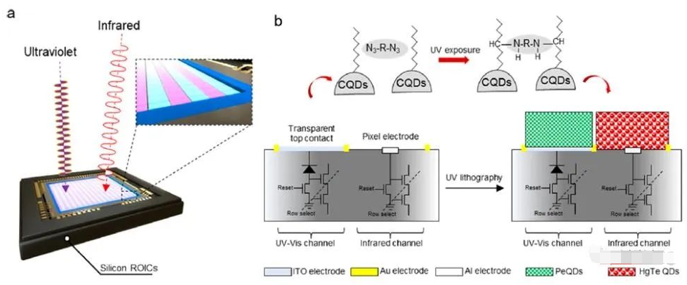
Fig. 1 a. Layout of the multi-band broad spectrum detector; b. Schematic diagram of the ligand exchange process and the structure of UV pixels and IR pixels.
The silicon-based readout circuit used in the multi-band broad spectrum detector was specially tailored and designed for the layout (Figure 1.a). One of the channels is a pixel modified with a transparent top electrode, which serves as a modified area for the chalcogenide quantum dots to respond to UV-band signals for the down-conversion process. The other channel is a pixel with a direct injection circuit as the acquisition and amplification circuit, in which mercury telluride colloidal quantum dot infrared material is modified to capture short-wave infrared signals from 1 to 2.5 μm and obtain the infrared characteristics of the object to identify the material composition (Figure 1. b).
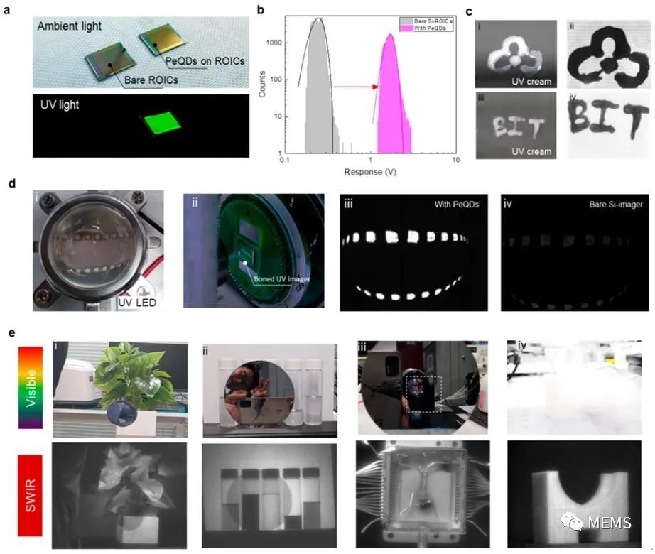
Figure 2 shows the detection effect graph of the multispectral broad-spectrum quantum dot detector made using this research method in monochromatic mode. In Figure 2.c, it can be seen that the sunscreen appears black under UV lamp irradiation, indicating that the UV light is absorbed by the sunscreen, and thus the UV signal is severely attenuated showing black in the area where the sunscreen is applied, also proving that the detection range of the detector in this mode is the UV band. Figure 2.e shows four classical scenarios in short-wave imaging. (i) (ii) (iii) shows that the short-wave IR can penetrate the silicon wafer because the absorption wavelength of the silicon wafer is up to 1.1 μm, while the detection range of the HgTe quantum dots used in the quantum dot detector is 1~2.5 μm, so the silicon wafer appears transparent in this detection band. A classical short-wave infrared application scenario is also shown in (ii) to discriminate the composition of chemicals. In the short-wave IR detection mode, transparent chemicals (from left to right: chlorobenzene, ethanol, chloroform, water, butyl acetate) show different gray levels in the picture due to the different absorption intensity of the short-wave by the chemical bonds they contain. (iv) shows the unique ability of imaging through clouds and fog at short wavelengths.
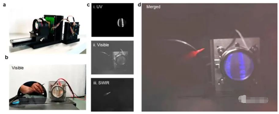
Figure 3 shows the use of a multispectral broad spectrum quantum dot detector to image a scene containing a soldering iron, silicon wafer and UV lamp at 580°C. It can be seen that the use of a multispectral broad spectrum quantum dot detector module is able to obtain the UV, visible and short-wave IR information features of the scene (short-wave IR information released by the soldering iron that can penetrate the silicon wafer, UV information released by the UV LED, wire and UV LED module visible light information), the fusion of images can show the spectral information from UV to short-wave infrared photos, providing more detailed information of the scene.

This research breakthrough can greatly simplify the optical hardware and software complexity of multi-band cameras, reduce the size and weight of the cameras, and help realize the micro-miniaturized platform design of multi-spectral cameras. The team uses direct lithography to realize colloidal quantum dots to realize two-color or multi-color focal plane arrays, breaking through the traditional block semiconductor material flip-flop bonding process to complete the multi-color detection coupling of detectors, realizing multi-band detection and multi-color imaging capability in a single detector, greatly reducing the cost of multi-color detector fabrication and improving the fabrication process scale and product qualification rate. (hereinafter referred to as “SMIC-Thermal”) in the preparation of focal plane detectors and testing of focal plane imaging systems. SMIC-Therm is the first high-tech enterprise focusing on infrared quantum material imaging chip field in China, focusing on new infrared quantum material device preparation and packaging technology, launching next-generation low-cost, high-resolution short-wave and mid-wave infrared imaging chip solutions around low-dimensional quantum materials, breaking through the traditional semiconductor flip-flop bonding process, and carrying out packaging and testing of low-cost silicon-based readout circuit-on-chip integrated infrared chips. business. At present, we have successfully developed 320×256, 640×512, 1280×1024 array scale short-wave infrared, mid-wave infrared and other focal plane array development work, and have batch production line design and production capacity.