Surface Mount Devices (SMDs) are now taking over the configurable logic market, especially the Printed Circuit Board (PCB) market. In the market, key packages like the TO263 bolster the performance of the target applications or devices.
This blog post explains what you need to know about working with the TO263, one of the most reliable semiconductor packages.
TO263 as a Standardized Semiconductor Package
Packing or packaging the content of the semiconductor components require careful handling, and that is where the TO263 comes in handy. The name “TO263” is only but a standardized format of the Double Decawatt Package (DDPAK), which refers to the doubled or dual semiconductor component package.
As the standardized format of the DDPAK or D2PAK, the TO263 helps to protect the semiconductor components of the target devices.
Worthy of pointing out is the fact that the TO263 standardized format is also known by other names, including:
- SOT404
- D2PAK
The Market Opportunity
Loopholes in the existing solutions tend to open up more opportunities for newer products and in this case, it is the TO263 semiconductor component package. The major market opportunity was the inability of the previous semiconductor package of the same family, called the DPAK to meet some of the industry standards.
The DPAK or Double Decawatt Package (DPAK) lagged in the area of improving the compatibility of the target devices with the semiconductor packages.
To add to this, the TO263 also solved one of the major challenges of the TO-220 semiconductor package, which is the absence of convenient mounting style, in the form of the mounting hole. The TO-220-styled semiconductor package also lacked an extended metal tab that could have bolstered the device’s heat or thermal dissipation.
TO263 as a DPAK Variant
To fix some of the lapses in the Double Decawatt Package (DPAK), the TO263 or DDPAK offers an improved design.
The design improvement is the package’s provision of larger real estate that favorably beats the compact design of the DPAK or TO-252 semiconductor package.
Technical Properties of the TO263 Package
Here are some of the technical properties or components of the Double Decawatt Package or TO263 semiconductor package.
1. Body Thickness
The body thickness of the TO263 package is 175 mils. The body thickness aligns with the terminal pitch, and can vary based on the number of terminals the package has.
For example, the 3-terminal TO263 package uses a 175 mils body thickness and a terminal pitch of 100 mils. Likewise, the 7-terminal TO263 uses a 175 mils body thickness and a terminal pitch and a terminal pitch of 50 mils.
The 5-terminal TO263 package, however, uses a terminal pitch of 67 mils on a 175 mils body thickness.
Despite the disparities in their body thicknesses and terminal pitch, the TO263 package maintains the same measurement for both the body size and the total length. The body size for the variants is 400 mils by 39 mils (the heatsink inclusive). The estimated measurement of the length (inclusive of the leads) is 600 mils.
2. TO263 Package is Encased for High-Power Discreet Devices
Motorola, the manufacturer of the TO263 package, optimized the package for use with the high-power discreet devices. These devices or applications are ideal for the following categories of high-power discreet devices or applications:
- Key applications or devices manufactured for the lightning, automotive and safety industries.
- High-power discreet applications, of up to 100A
- DC-to-DC converters
- Low on-resistance MOSFETs
- Power supply circuits
- High-speed switching MOSFETs
Categories of the TO263 Semiconductor Package
You need to understand that the TO263 has several variants, with each of them offering specific values to the overall functionalities of high-power discreet applications.
Although the variants are typically narrowed down to the TO263-3 and the TO263-7 packages, there are many other variants you must know.
Below are some of the popular variants of the TO263, including how each of those varying semiconductor packages work:
1. TO263-3
It is one of the most popular variants of the TO263. It is so-named because of the composition of three (3) pins. Just like most of the other semiconductor packages out there, the TO263-3 uses the last number of the package to specify the number of pins it has.
One major attribute of the TO263-3 DDPAK variant is that it is based on the standard JEDEC 2-layer and 4-layer Printed Circuit Boards (PCBs).
TO263-3 variant also has a special consideration for further variations, which is the reason why it offers the Three-Dimensional (3D) models of the package. An example is the TO263-3S.
2. TO263 THIN
This TO263 variant is named this way because of the “thin” or smaller footprint. Typically, its thinner or smaller Printed Circuit Board (PCB) footprint is derived from the significantly smaller height.
Texas Instruments manufactures the TO263 THIN D2PAK variant and makes it compatible to the standard TO263 semiconductor package via the addition of the exposed pad underneath the package.
3. TO263-5
TO263 is the 5-pin variant of the broader DDPAK package. It also has a 3D model, which is the TO263-5S.
The variant maintains a “no flow” thermal resistance, highlighted by the 22.0-degree Celsius/W based on the JEDEC 4-layer test circuit board.
Common Features of the TO263 Semiconductor Package

Below are some of the common attributes or properties of the TO263/DDPAK semiconductor package:
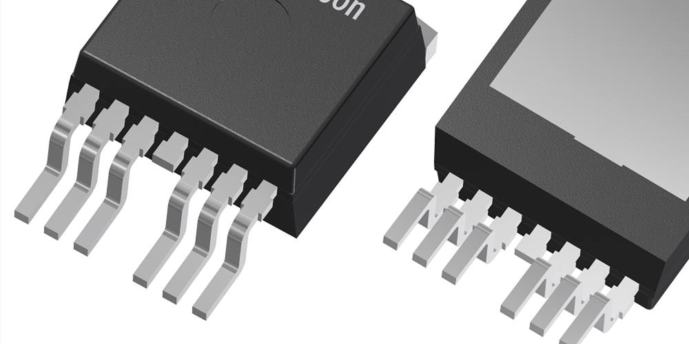
1. SMD Design
TO263 is sometimes referred to as the “SMD-220” meaning that it is the Surface Mount Technology (SMT) variant of the TO-220 semiconductor package, which uses the Through-Hole Technology (THT).
2. Pitch and Height Variations
The pitch and height of the TO263 varies by several factors. For example, the TO263 THIN variant maintains a package height of 4.57mm, a combination of Length, Width and Height (L, W, H).
The pitch of the packages also varies by the variations, such as the TO263-3 and TO263-3S having a pitch of 2.54mm and the TO263-7 and TO263-7S variants having a pitch of 1.7mm.
3. Thermal Pad Composition
The thermal pad of the TO263 (or any semiconductor package at all) is the primary medium for transferring or conducting heat or thermal energy from the package into the circuit board.
Both the standard TO263 package and the other variants of the package have a thermal pad, typically located underneath the package.
Conclusion
TO263 is a standardized semiconductor package for Surface Mount Devices (SMDs) optimized for high-power, discreet applications. Pick from any of the variants and get started with improving the heat/thermal energy/power dissipation of the power-centric applications.