Saving costs when working on a Printed Circuit Board (PCB) has become one of the factors to consider when working on the board. To get value for money, consumers are now turning their attention to Integrated Circuit (IC) packages with cost-saving features. PLCC is one of such packages.
The interesting thing about this IC package is that it is generally considered to be the cheaper variant of the CLCC IC package. This article exposes everything you need to know about PLCC.
What is the Meaning of PLCC?
It means Plastic Leaded Chip Carrier PLCC. The three keywords to take out of that are:
- Plastic, meaning that the IC package is made of some plastic materials.
- Leaded, meaning that it does use leads.
- Chip carrier, which means that PLCC provides chips needed for connecting the package to the circuit board.
PLCC is a one of the IC packages categorized under Surface Mount Devices (SMDs). Its plastic and leadless composition enable the use of the sided connection leads to connect either to the PLCC sockets or soldered to the circuit board.
Design of the PLCC
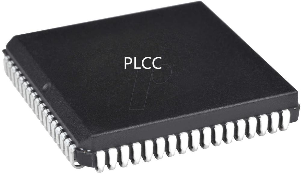
PLCC takes on a rectangular or square shape and has the “J-lead” design. The lead design takes root in the strategic positioning of the leads in the form of a J. Also, the “J-lead” design extends to the lower section of the package, which folds towards the back.
Integration Options
Integrating or adding the PLCC to the Printed Circuit Board (PCB) can be done with either the PLCC socket or the soldering format.
Worthy of mentioning is that the “J-lead” design buoys the multiple integration options, especially for the soldering. Using the soldering option appears to be a better option for several reasons. With it, the PLCC IC package will not only be placed in real-time on the circuit board, but can also be removed with ease when it gets damaged.
On the flipside, soldering the PLCC to the circuit board may also pose a challenge – exposing the chip to (excessive) heat. Therefore, sticking to the PLCC socket appears to be a better option.
Using the PLCC socket involves handily or manually attaching the PLCC IC package to the PLCC socket. The socket then holds the package in place and prevents the chip inside the carrier from getting damaged during the mounting process.
The Possibilities of Programming the PLCC
Soldering the PLCC or using the PLCC socket for the same appear to be the most popular. However, there is a third option – programming the package.
It should come third on the list and only considered after the other (two) options have been explored.
Programming a PLCC IC package requires an independent programming of the package before connecting it to the Printed Circuit Board (PCB). Note that the programming works best if the package is inside a Programmable Logic Device (PLD).
Benefits of the PLCC IC Package
Get the most out of the package by taking a look at some of the advantages it has to offer. Here they are:
1. Off-Board Programming
While most Integrated Circuit (IC) packages require on-site integration, PLCC allows for external programming.
If you are working on a PLD chip, it is possible to take the PLCC package out of the circuit board and program it before insertion.
Also, the off-board programming is essential for making future firmware updates and subjecting the package to performance testing, especially for circuit board prototypes.
2. Space Efficiency
Maximizing the available space is one of the core attributes PLCC has. The “J-lead” design helps to accommodate as many components as possible, as it folds into a heel to give the “J” shape.
3. Real-Time Damage Assessment and Fixing
PLCC’s “J-lead” design with a heel folding format compares to the Quad Flat Package’s toe folding format.
The “J-lead” design allows for the easier assessment of damages to the chip, especially if the PLCC socket was used when inserting it.
Also, it is easier to remove the PLCC from the PCB and replace it with a new one, with decoupling the entire board.
We think this is a better alternative to the gull-wing leaded QFP that may require reopening and reconstruction of the entire circuit board when the chip damages.
4. Excellent Thermal Resistance
Excessive heat, when exposed to the chip, may damage the latter. To address this, the PLCC IC package uses a PLCC socket first before adding the chip, which has been programmed off-site.
Doing that prevents the chip from getting exposed to excessive heat and at the same time, boosts the overall system reliability of the circuit board.
5. Small Form Factor
PLCC IC package derives its small form factor design from the “J-lead” design that allows for a significant reduction of real estate usage.
By reducing the PCB footprints, the package can considerably avoid the need for x-ray inspections, which are common for the Quad Flat Packages (QFPs).
PLCC vs. LCC IC Packages: The Differences between the Two

Plastic Leaded Chip Carrier (PLCC) has been compared to the Ceramic Leadless Chip Carrier (CLCC).
This section covers the major differences between the two.
1. Cost
The primary difference between the PLCC and the CLCC IC packages is how much it takes to get any of them. Generally, the PLCC is considered to be a cost-effective variant of the CLCC both because of the well-optimized real estate usage and the affordability of the (plastic) component.
2. Susceptibility to Damages
PLCC IC package can be inserted into the circuit board with variety of options, including soldering, off-site programming and using a PLCC socket.
It is less susceptible to damages when programmed off-site or inserted with the help of the PLCC socket. That helps to protect the chip. Even if the chip were to get damaged, it can simply be removed and replaced, rather than working on it.
Conclusion
Plastic Leaded Chip Carrier (PLCC) is a better alternative to the Ceramic Leadless Chip Carrier (CLCC), because of the affordability, flexible design and small form factor. Although the CLCC gets more used because of the adaptability, it doesn’t give the users several configuration options – and it can be a bit on the high-end side.