XC7K70T-2FBG484C ApplicationField
-Wireless Technology
-Artificial Intelligence
-Cloud Computing
-Consumer Electronics
-Medical Equipment
-Internet of Things
-Industrial Control
-5G Technology
Request XC7K70T-2FBG484C FPGA Quote , Contact Sales@ebics.net Now
XC7K70T-2FBG484C FAQ

Q: Does the price of XC7K70T-2FBG484C devices fluctuate frequently?
A: The EBICS search engine monitors the XC7K70T-2FBG484C inventory quantity and price of global electronic component suppliers in real time, and regularly records historical price data. You can view the historical price trends of electronic components to provide a basis for your purchasing decisions.
Q: What should I do if I did not receive the technical support for XC7K70T2FBG484C in time?
A: Depending on the time difference between your location and our location, it may take several hours for us to reply, please be patient, our FPGA technical engineer will help you with the XC7K70T-2FBG484C pinout information, replacement, datasheet in pdf, programming tools, starter kit, etc.
Q: Where can I purchase Xilinx XC7K70T Development Boards, Evaluation Boards, or Kintex-7 FPGAs Starter Kit? also provide technical information?
A: EBICS does not provide development board purchase services for the time being, but customers often consult about ZedBoard, Basys 3 board, TinyFPGA BX, Nexys4-DDR, Terasic DE10-Nano, Digilent Arty S7, etc. If you need relevant technical information, you can submit feedback information, our technicians will contact you soon.
Q: Do I have to sign up on the website to make an inquiry for XC7K70T-2FBG484C?
A: No, only submit the quantity, email address and other contact information required for the inquiry of XC7K70T-2FBG484C, but you need to sign up for the post comments and resource downloads.
Q: How can I obtain software development tools related to the Xilinx FPGA platform?
A: In FPGA/CPLD design tools, Xilinx’s Vivado Design Suite is easy to use, it is very user-friendly in synthesis and implementation, and it is easier to use than ISE design tools; The specific choice depends on personal habits and functional requirements to specifically select a more suitable match. You can search and download through the FPGA resource channel.
Q: How to obtain XC7K70T-2FBG484C technical support documents?
A: Enter the “XC7K70T-2FBG484C” keyword in the search box of the website, or find these through the Download Channel or FPGA Forum .
XC7K70T-2FBG484C Features
Designed for high performance and lowest power with 28 nm, HKMG, HPL process, 1.0V core voltage process technology and 0.9V core voltage option for even lower power.
36 Kb dual-port block RAM with built-in FIFO logic for on-chip data buffering.
A user configurable analog interface (XADC), incorporating dual 12-bit 1MSPS analog-to-digital converters with on-chip thermal and supply sensors.
Wide variety of configuration options, including support for commodity memories, 256-bit AES encryption with HMAC/SHA-256 authentication, and built-in SEU detection and correction.
Low-cost, wire-bond, lidless flip-chip, and high signal integrity flipchip packaging offering easy migration between family members in the same package. All packages available in Pb-free and selected packages in Pb option.
Advanced high-performance FPGA logic based on real 6-input lookup table (LUT) technology configurable as distributed memory.
DSP slices with 25 x 18 multiplier, 48-bit accumulator, and pre-adder for high-performance filtering, including optimized symmetric coefficient filtering.
High-speed serial connectivity with built-in multi-gigabit transceivers from 600 Mb/s to maximum rates of 6.6 Gb/s up to 28.05 Gb/s, offering a special low-power mode, optimized for chip-to-chip interfaces.
High-performance SelectIO™ technology with support for DDR3 interfaces up to 1,866 Mb/s.
Powerful clock management tiles (CMT), combining phase-locked loop (PLL) and mixed-mode clock manager (MMCM) blocks for high precision and low jitter.
Integrated block for PCI Express® (PCIe), for up to x8 Gen3 Endpoint and Root Port designs.
Request XC7K70T-2FBG484C FPGA Quote , Contact Sales@ebics.net Now
XC7K70T-2FBG484C Overview
Xilinx® 7 series FPGAs comprise three new FPGA families that address the complete range of system requirements, ranging from low cost, small form factor, cost-sensitive, high-volume applications to ultra high-end connectivity bandwidth, logic capacity, and signal processing capability for the most demanding high-performance applications. The 7 series FPGAs include:Artix®-7 Family: Optimized for lowest cost and power with small form-factor packaging for the highest volume applications.Kintex®-7 Family: Optimized for best price-performance with a 2X improvement compared to previous generation, enabling a new class of FPGAs.Virtex®-7 Family: Optimized for highest system performance and capacity with a 2X improvement in system performance. Highest capability devices enabled by stacked silicon interconnect (SSI) technology.Built on a state-of-the-art, high-performance, low-power (HPL), 28 nm, high-k metal gate (HKMG) process technology, 7 series FPGAs enable an unparalleled increase in system performance with 2.9 Tb/s of I/O bandwidth, 2 million logic cell capacity, and 5.3 TMAC/s DSP, while consuming 50% less power than previous generation devices to offer a fully programmable alternative to ASSPs and ASICs.
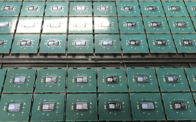
The Xilinx FPGAs (Field Programmable Gate Array) series XC7K70T-2FBG484C is FPGA, Kintex-7, MMCM, PLL, 185 I/O’s, 710 MHz, 65600 Cells, 970 mV to 1.03 V, FCBGA-484, View Substitutes & Alternatives along with datasheets, stock, pricing from Authorized Distributors at EBICS.com,
and you can also search for other FPGAs products.

XC7K70T-2FBG484C Tags
XC7K70T development board
Xilinx XC7K70T
Xilinx Kintex-7 FPGAs development board
XC7K70T evaluation board
Kintex-7 FPGAs evaluation kit
XC7K70T reference design
Kintex-7 FPGAs XC7K70T
Kintex-7 FPGAs starter kit
XC7K70T-2FBG484C TechnicalAttributes
-Package / Case 484-BBGA, FCBGA
-Mounting Type Surface Mount
-Total RAM Bits 4976640
-Number of I/O 285
-Voltage – Supply 0.97V ~ 1.03V
-Supplier Device Package 484-FCBGA (23×23)
-Operating Temperature 0℃ ~ 85℃ (TJ)
-Number of LABs/CLBs 5125
-Number of Logic Elements/Cells 65600
-Number of LABs/CLBs 5125
Request XC7K70T-2FBG484C FAQ Quote , Pls send email to Sales@ebics.net or Submit form now
Related posts:
- XCZU7EG-2FFVC1156I Xilinx XCZU7EG XCZU7EG evaluation board
- XCZU21DR-2FFVD1156I Xilinx Zynq UltraScale+ RFSoC development board XCZU21DR reference design
- XCZU7CG-2FFVF1517I XCZU7CG development board XCZU7CG-2FFVF1517I Datasheet PDF
- XC7Z035-L2FFG676I XC7Z035-L2FFG676I Datasheet PDF Xilinx Zynq-7000 SoC development board
