With the rapid development of a new generation of information and communication technology, as a terminal device, smart phones, tablet PCs, smart homes and other products, the market demand continues to grow, LCD panel production scale has increased dramatically, becoming one of the pillars of the information industry. The rise of the LCD panel industry has led to a surge in demand for panel quality inspection. Traditional defect detection is mainly identified by the human eye, which brings great difficulties to enterprises to control production quality and improve production efficiency. In view of this, the adoption of a new panel quality inspection method to replace manual inspection is an urgent technical problem to be solved.

01 LCD panel defects from the origin
Thin film transistor liquid crystal display (TFT-LCD) has the advantages of high resolution and low power consumption, so it is widely used in the display industry. The production process of TFT-LCD display includes coating, etching, developing, panel combination, crystal filling and sealing, and driver chip installation, etc. The complex process leads to defects, including point defects, line defects and Mura defects. The word “Mura” comes from Japanese and translates to spot, dirt, also known as “cloud spot”, which is one of the most difficult defects to detect in display defects. The traditional Mura inspection method is achieved by manual visual inspection, mainly by naked eye discrimination. This method is inefficient and prone to visual fatigue, which leads to a lower correct result rate. Machine vision-based LCD panel inspection can be realized to detect defects generated by each production process of LCD panels, including Array (array) process, CF (color film) process, CELL (boxing) process, Module (module) process, crack (crack), broken (broken), chip (chipped), scratch (scratch), burr (burr). We can effectively detect and distinguish defects such as crack, broken, chip, scratch, burr and drop.
02 LCD panel inspection difficulties
Product area of high capacity, manual can not do every sheet detection, the risk of leakage
LCD panels are usually very large before they are cut, and in the case of a 10.5 generation line, for example, the entire panel area can reach
3370mm*2940mm, manual inspection is extremely difficult and easily fatigued, and the capacity and accuracy cannot be guaranteed by manual inspection.
Panel defects are very likely to lead to broken products
LCD panel production process will be probable chipping, breakage, cracks, scratches and other defects, if not found and dealt with in a timely manner, into the next production process of the main equipment, may occur during the production process in the equipment inside the glass breakage phenomenon, so that the main equipment must be shut down for maintenance and cleaning, resulting in economic losses of production downtime.

The location and type of defects cannot be statistically summarized and analyzed, and cannot be digitized.
Manual testing without picture and image data records, poor consistency of testing standards, can not be traced back to the product.
Difficult to recruit workers and high labor costs
As the per capita wage level continues to increase, the cost of employing people is also rising year by year, and the difficulty of recruiting and the mobility of personnel. And manual testing is more harmful to the eyes, resulting in a high mobility of personnel and certain difficulties in recruiting.
03 LCD panel inspection method
In recent years, many computer vision-based panel defect detection systems have emerged, but the defect detection algorithms utilized by various manufacturers are basically more traditional vision methods. However, as the production process continues to progress, the detection requirements are subsequently increased, the detection accuracy requirements are also increasing, and the real-time requirements for the algorithms are greatly improved. With the rise of deep learning, for such difficult-to-detect defects, we use convolutional neural networks (CNN) for the detection of screen defects. For the detection problem, there are many existing target detection algorithms that can achieve higher accuracy and real-time detection, effectively identifying and classifying LCD panel defects – achieving defect detection for chipped edges, cracks, dirt, water drops, scratches, etc., and interfacing with the main production equipment, detecting defects and then automatically making, according to the type of defect Feedback judgment: stop or alarm, no need for real-time monitoring by staff on site.
Increase efficiency
Deep learning algorithms can identify production hazards such as chipped edges more accurately, i.e. eliminating production line downtime due to glass fragments and false alarms due to misidentification, thus improving production efficiency.
Cost reduction
Avoid equipment damage caused by glass breakage, reduce the cost of lost work due to equipment downtime, and also reduce the cost of equipment maintenance.
Upgrade quality
Reduces product quality problems due to surface scratches and dirt affecting circuit production and LCD imaging.
Lift process
Through the digitization of quality inspection, the ability of data traceability analysis is improved, which provides a strong guarantee for improving the production process.
LCD screen appearance defect detection program
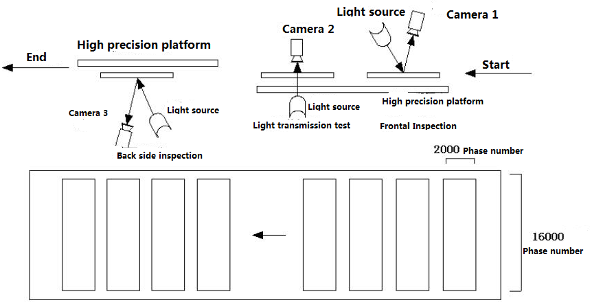
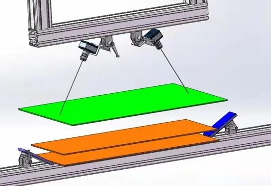
Using line array camera, lens, according to the detection demand items, choose to match the backlight, coaxial light or high bright line light source for LCD panel image acquisition, in the process of scanning pictures, intelligent algorithms simultaneously processing images, real-time display of the panel defect information, determine whether the surface has foreign objects, scratches, different colors, convex bags, dents, pinholes, burrs, bright spots, for defective glass, real-time linkage of the main equipment to stop and other related operations to prevent the main equipment downtime due to broken glass in the production process.
Machine vision inspection process design.
1、Open the product into 180°, place the LCD screen horizontally on the carrier table; 2、Start inspection: the carrier table moves and the camera starts to acquire images; 3、After the acquisition, the carrier table is reset; 4、Inspection software: analyze the quality of the LCD screen; 5、According to the analysis result, give the OK and NG evaluation result of the product; 6、Operator: according to the result, carry out binning operation and reinspection operation;
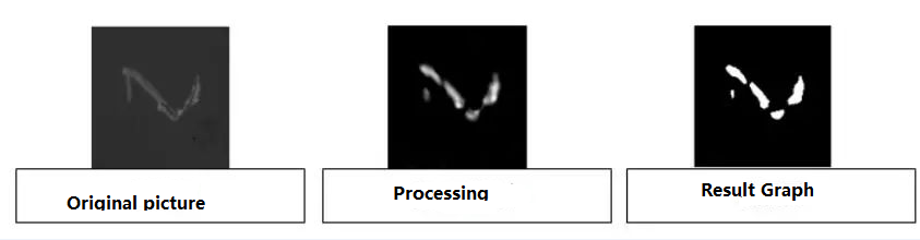
A) Visual detection of abnormal black spots

B) Visual detection of abnormal foreign objects
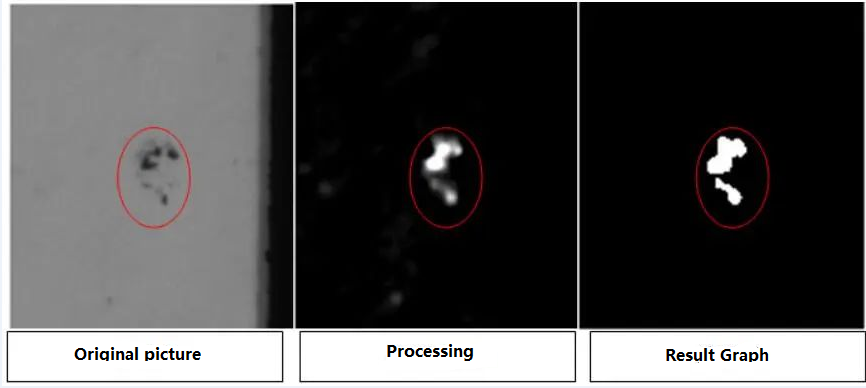
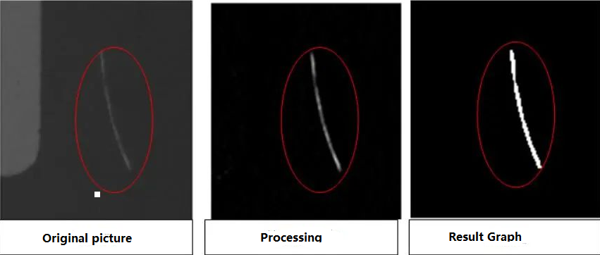
C) Visual inspection of abnormal scratches
D) Visual detection of abnormal bubbles

E) Visual detection of abnormal foreign objects