GaN-on-Si is a disruptive semiconductor technology that is coming of age. GaN-on-Si technology is a manufacturing process that grows GaN devices directly onto a conventional silicon substrate. In this process, low cost, high volume production of GaN devices can be achieved using the existing silicon-based semiconductor manufacturing infrastructure as the GaN film is grown directly on the silicon substrate.
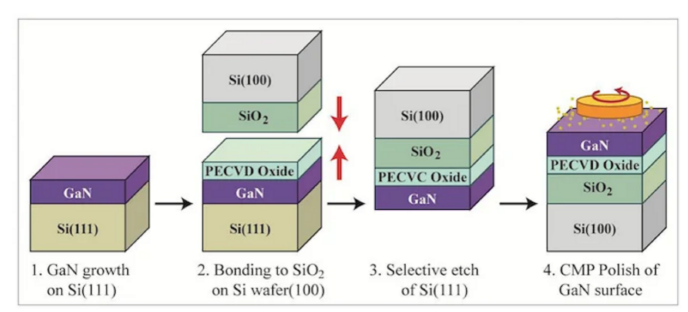
A schematic of the GaN-on-Si manufacturing process flow is shown in the diagram. Like the manufacture of an atomic bomb, the principle may seem simple, but the process is not without its challenges. The difference in lattice constants between the two materials has proven to make it extremely difficult to grow high quality GaN films from silicon substrates due to the severe lattice mismatch that can occur. For this reason, GaN-on-Si technology is not yet widely used in RF applications. With the continued injection of R&D funds into the technology by industry leaders such as STMicroelectronics and Magnesium, GaN technology is set to become one of the most promising emerging technologies.
GaN-on-Si performance offers power efficiencies in excess of 70%, increases power per unit area by a factor of 4 to 6, and scales to high frequencies. GaN-on-Si is used as an electrical insulator in power IC chips. Its “green” properties include an extremely low carbon footprint due to its aluminium source. The use of GaN in these power IC chips saves up to 80% of the manufacturing and packaging process and also provides significant improvements in system-level efficiency.
The GaN-on-Si process is highly energy dense and reliable, and wafers can be made very large, currently at 8 inches and in the future at 10 inches and 12 inches, with wafer lengths of up to 2 metres. GaN-on-Si devices have the advantages of high breakdown voltage, low on-resistance, fast switching speed, zero reverse recovery charge, small size and low energy consumption, and radiation resistance. The theoretical chip area for the same breakdown voltage and on-resistance is only one thousandth of that of silicon, and is currently capable of one-tenth.

If there is any drawback to GaN-on-Si devices, it is the cost and size. However, we understand that the cost of the supporting peripheral electronics and cooling system required is significantly reduced with the use of such devices. Although GaN is more expensive than silicon-based devices in terms of individual device cost, the overall system cost difference between GaN and silicon-based devices is already very small, and in mass production it is possible to achieve higher performance and lower cost than silicon devices.
GaN-on-Si applications
In terms of RF energy, due to the heating nature of microwave radio frequency, GaN can be used in more industrial and lifestyle applications, including RF cookware, RF dryers, RF lighting, spark plugs and even intelligent agricultural lighting. In terms of data communication, the cost of PA currently accounts for roughly 40% of the entire base station signal link, so the cost of PA directly affects the overall system cost. In addition to cost reduction through capacity enhancement, large-scale integration is also the future demand, especially for the 64 or even 128 links corresponding to 5G MIMO, integration is the key, the future CMOS process of GaN-on-Si MMIC will definitely have market potential