Last month to do resistive resistance method of blood cell counting (also known as Coulter principle) pre-research, consider using the instrumentation amplifier to try the effect, because its common mode rejection ratio CMRR very high such as low frequency to 60Hz can reach 120dB; the actual test effect is not bad. Now this project has been stopped …… but still took this opportunity to basically figure out the principle of input and output limiting of the instrumentation amplifier, will use ADI’s diamond diagram tool simulation. Therefore, the content of this article is to apply the knowledge learned, on a very common PT100 bridge circuit, using ADI instrumentation amplifier online tool diamond diagram to assist in the design process.
Design objectives.
- PT100 temperature measurement limit of 0 ℃ ~ 150 ℃; 2. power supply 0 ~ 5 V; 3. PT100 amplifier circuit output for 0 ~ 2.5V between, because the quantization device ADC reference source for the common 2.5V; 4. the board can work in -40 ℃ ~ 80 ℃. These design input conditions are sufficient to complete the verification of the instrumentation amplifier input and output.
Circuit diagram.
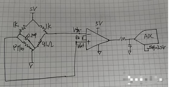
Figure 1 PT100 amplifier circuit
Instrumentation meter amplifier input and output limitations analysis.
From the design conditions in the design objectives, we are able to calculate the Vdiff minimum and maximum values, the Vcm minimum and maximum values, and the gain of the instrumentation amplifier so that we can simulate the input and output limits using the diamond diagram tool.
Vdiff_min = Vin+_min – Vin- = 0.0375V
Vdiff_max = Vin+_max – Vin- = 0.2629V
Vcm_min = (Vin+_min + Vin-) / 2 = 0.4357V
Vcm_max = (Vin+_max + Vin-) / 2 = 0.5484V
By substituting the above four equations for the values of the individual devices in the circuit diagram, the minimum and maximum values of Vdiff and Vcm can be calculated respectively.

From Vdiff_max = 0.2629 and Vout is limited to between 0 and 2.5V, we can also calculate that the gain can be 8.
Here we can select a random ADI instrumentation amplifier and use the diamond diagram tool to analyse whether its input and output limits meet the requirements, see Fig. 2. From the results in Fig. 2 we can see that the red box is not in the white area of the diamond diagram and an exclamation mark appears, indicating that there is a problem with the circuit. In the bottom left hand corner the cause of the problem and suggestions for changes are given. In the upper column is the option “Internal circuit”, which we can click on to find out what is wrong, see figure 3.
From this, we can also see why the input and output limits of the instrumentation amplifier require a special tool to simulate it more easily, as the internal architecture contains three op-amps and a reference voltage input, all of which are related to its input and output limits; unlike the op-amps, which can be found by simply checking the datasheet. The recommended devices are listed in the top column of Figure 2, so that we can replace the op-amp directly without changing the circuit configuration to solve the problem, and choose any of these recommended devices to meet the requirements.
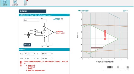
Figure 2 Results of the diamond diagram analysis of the AD8226 as an amplifier in the circuit
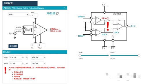
Figure 3 The Diamond Diagram tool allows you to see where limits are exceeded by looking at the internal circuit
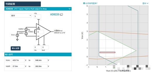
Figure 4 The Diamond Diagram simulation tool no longer reports errors after replacing the op-amp
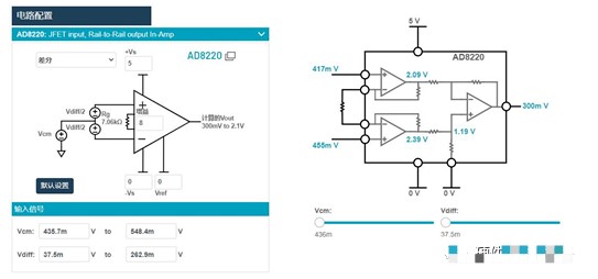
Figure 5 Node voltage inside the internal chip after replacing the op-amp
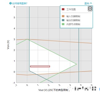
Figure 6 Meaning of the various coloured lines
Finally, one of the design conditions is that the circuit has to operate normally within -40~80°C, so we have to leave a margin in our design to do so. After checking the AD8220 datasheet, we found that it does not have data on the variation of voltage at each node with temperature and calculation formulae similar to the AD8226, so we can only design with margins, usually several hundred millivolts for the full temperature range. From the simulation results of the diamond diagram, the red box is close to the output limit, so if you are conservative, you can turn down the gain, for example to 7, and pull the red box away from the output limit.
Translated with www.DeepL.com/Translator (free version)