Explain one type of full-bridge circuit: the full-bridge inverter circuit
In accordance with past habits, the original route map will be shown first.
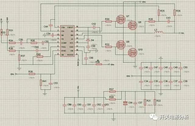
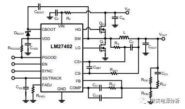
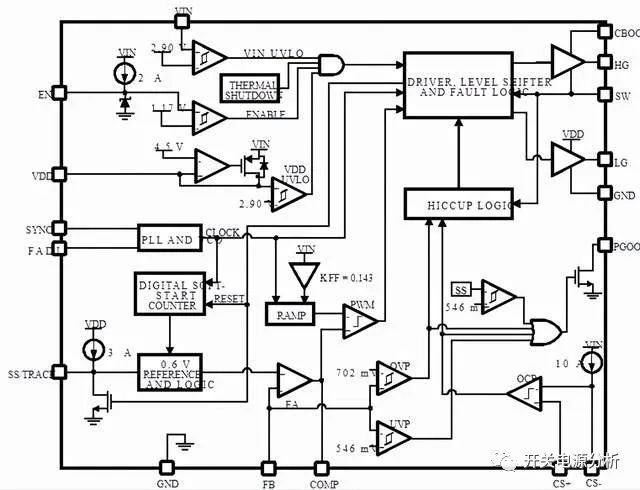
We can see the above diagram is a full-bridge switching power supply output part of the chip and 4 MOS tubes together, the chip used at the time seems to be LM27402MHX model, specific parameters interested partners can look up online, I only posted the chip manufacturer recommended peripheral circuit architecture diagram and chip internal structure of the original circuit diagram, as shown below.
First, the external power supply voltage to the chip pin 12 to provide a stable DC supply voltage, many of our chips are in the 14V supply voltage, but the maximum supply voltage of this chip only allows 6V, so in the design to pay attention to the chip power supply design, otherwise it is very easy to cause the chip burn phenomenon, before we design is because we are too confident, did not read the specifications of the chip supply voltage, resulting in the burning of three chips, and later investigated a long time to find the cause, so this should pay special attention to.

First, the external supply voltage to the chip pin 12 to provide a stable DC supply voltage, we have many chips in the supply voltage of about 14V, but the maximum supply voltage of this chip only allows 6V, so in the design of the chip power supply design, otherwise it is very easy to cause the chip burn phenomenon, before we design is because we are too confident in their own, did not read the specifications of the chip supply voltage, resulting in the burning of three chips, and later investigated a long time to find the cause, so this should pay special attention to.
When the supply voltage condition is met, the voltage will pass through the diode D4 to the bootstrap capacitor C42 charging operation, C42 voltage rise, the chip internal voltage to C53 and C54 charging, so that the chip enable pins and soft start pins voltage rise, the chip for the first start, the output corresponding pulse signal to the MOS tube gate, MOS conduction, the output DC voltage, the voltage is filtered by the back stage capacitor. The voltage is filtered by the rear capacitor to get a smooth output voltage, this voltage is input to the voltage feedback pin of the chip through R33 and R36, the chip internal voltage detection operation, if the voltage is too high or too low will cause the chip to protect the operation; thus leading to the product can not be normal output, if the output voltage is normal, the chip will work, the chip pin 15 and pin 13 respectively output High and low levels to the MOS tube gate, we can see Q7 and Q8 on at the same time, Q9 and Q10 on at the same time, and Q7Q8 on time and Q9Q10 must be staggered, there can be no overlap, otherwise the product will enter the dead zone, resulting in the product components too much energy and burned. Q7Q8 on time and Q9Q10 must be staggered, there can be no overlap, otherwise the product will Q7Q8 conduction time and Q9Q10 must be staggered, not to overlap, otherwise the product will enter the dead zone, resulting in excessive energy of the product components and burn.
This chip has an internal output overvoltage protection function OVP, output undervoltage protection function UVP, output overcurrent protection function OCP; input overvoltage and undervoltage protection function; interested partners can try to build the line architecture of this chip by themselves.