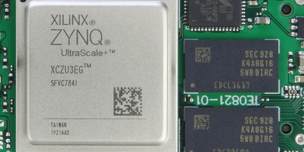
Xilinx Zynq is a processing platform based on APSOC. The essential feature of this FPGA is to incorporate a programmable FPGA chip and a dual-core ARM Cortex-A9 processor in a system-on-chip. The processing system of this FPGA comprises ARM processor and storage peripheral resources. However, the FPGA part is the programmable logic.
What is Xilinx Zynq?
Xilinx Zynq is an FPGA family developed according to the Xilinx SoC architecture. These FPGAs incorporate a dual-core or single-core ARM Cortex A9 based processing system. The heart of the processing system is the ARM Cortex-A9 CPUs. Also, the memory interfaces, peripheral connectivity interfaces and the on-chip memory are crucial in this FPGA.
Also, ARM Cortex-A9 supports performances similar to Linux operating system. The architecture of Xilinx Zynq integrates the AXI interface of the industry. Therefore, this creates a great coupling between the FPGA and ARM. As a result, this minimizes additional power consumption of discrete chips. Also, it helps to achieve low-latency connections and as well reduces the production cost and physical size.
The soft processor MicroBlaze can configure the programmable logic of Xilinx Zynq. Also, MicroBlaze consists of programmable logic units. This means that the deployment and integration of a MicroBlaze is similar to an FPGA IP core. Also, the soft processor can coordinate certain underlying functions. The programmable logic (PL) of Xilinx Zynq helps to discover the subsystem of high-speed logic operation.
Furthermore, the processing system (PS) supports operating system or software control. Therefore, you can divide most system designs into hardware and software-based functions. This enables the programmable logic and processing system to play their crucial roles. Therefore, the entire system will display the best performance.
What does Xilinx Zynq Offer?
Xilinx Zynq provides the scalability and flexibility of an FPGA while delivering great performance and power. The efficient power and performance of Xilinx Zynq is usually associated with ASSPs and ASIC. Also, the Xilinx Zynq family features a wide range of devices that enable designers to offer solutions to cost-sensitive and high-performance applications.
Every device in Xilinx Zynq family comprises the same I/O resources, PL, and PS. However, these elements may vary between the devices. Therefore, the Xilinx Zynq is ideal for use in a vast range of applications like medical diagnostics and imaging, broadcast camera, and Multifunction printers. Also, this FPGA is commonly used in machine vision, industrial networking, and industrial motor control.
Xilinx Zynq architecture allows the integration of custom software in the PS and custom logic in the PL. Therefore, this helps to realize differentiated system functions. The implementation of the PL with the PS offers performance levels that can’t be matched by two-chip solutions. This is because of their low latency, limited I/O bandwidth, and low power budgets.
Furthermore, Xilinx Zynq provides a vast number of soft IP. Also, the Linux drivers are available for the peripherals in the programmable logic and processing system. The development environment of Vivado Design Suite allows quick product development for systems engineers. Also, the implementation of the ARM-based PS offers a wide range of third-party tools.
The application processor included in this FPGA allows high-level operating system support. The PL and PS have their separate domains. Therefore, they enable the user to power down the PL when power management is necessary. The processor in the PS will boot first. Therefore, this enables a good approach for PL configuration. Also, the software running on the CPU manages PL configuration. Therefore, it boots like an ASSP.
The Processing System of Xilinx Zynq
The processing system of Xilinx Zynq consists of four blocks which are:
- I/O peripherals
- Application processor unit (APU)
- Memory interfaces
- Interconnect
I/O peripherals
The I/O peripherals feature the data communication peripherals. Also, these peripherals feature two USB 2.0 OTG peripherals that support about 12 endpoints individually. Therefore, this supports full-speed and high-speed modes in On-The-Go configuration. I/O peripherals relate with external devices via a shared pool of about 54 dedicated multiuse I/O pins.
Application processor unit (APU)
The APU comprises single-core or dual-core ARM Cortex-A9 MPCores. Also, the APU can function in single processor, asymmetric dual processor modes, and symmetric dual processor. This unit features an accelerator coherency port (ACP) interface that allows accesses from PL to CPU.
Memory interfaces
This unit offers static memory interface modules and dynamic memory interface modules. Also, the dynamic memory controller supports LPDDR2, DDR3, DDR2, and DDR3L memories. However, the static memory controllers offer support to a Quad-SPI flash interface and a NAND flash interface. Also, they support a parallel NOR flash interface and a parallel data bus.
You can configure the multi-protocol DDR memory controller to offer 32-bit and 16-bit accesses to a 1 GB address. The processing system integrates the associated PHY and the DDR controller. Also, the DDR memory controller enables the PL and PS to access a common memory.
Interconnect
The IOP, APU, and memory interface unit are all linked to each other and to the PL. This is possible through a multilayered ARM AMBA AXI interconnect. Also, this non-blocking interconnect support multiple master-slave transactions that occur simultaneously.
The interconnect features latency sensitive masters like ARM CPU. Therefore, it has the shortest paths to bandwidth masters like the PL masters.
The Programmable Logic of Xilinx Zynq

The programmable logic of Xilinx Zynq comprises the following
- Block RAM
- CLB
- Low-power serial transceivers
- Programmable I/O blocks
- DSP slices
- XADC (Analog-to-digital converter)
Configurable logic block (CLB)
The CLB architecture features some key features like 6-input LUTs, register and shift register functionality. Also, it features memory capability within the Look-up Tables (LUTs). Also, you can configure LUTs to be two 5-input LUTs or a one 6-input LUT. You can register each LUT output optionally in a flip-flop. A slice features four LUTs, eight flip-flops as well as arithmetic carry logic and multiplexers. The configurable logic block comprises two slices.
Block RAM
The Block RAM is an important element in programmable logic. Also, Block RAM features built-in optional error correction circuitry and programmable FIFO logic. Furthermore, it features a dual-port 36 Kb block RAM with about 72 port widths. Every device in the Xilinx Zynq comprises about 755 dual-port block RAMs. Every block RAM includes two independent ports that share the stored data.
Low power serial transceivers
The low power transceivers feature a high-performance GTX transceivers with about 12.5 Gb/s line rates. The GTP transceiver has about 6.25 Gb/s featuring wire-bond packages. Also, there is the low-power mode for chip-to-chip interfaces. The transceiver counts are between 0 to 16 transceiver circuits. Every serial transceiver features a combined receiver and transmitter.
The different serial transceivers can combine LC tank and ring oscillators architecture. This enables a great blend of performance and flexibility while allowing IP portability across family members. You can achieve lower data rates by utilizing logic-based oversampling. The serial receiver as well as transmitter are independent circuits that integrate advanced PL architecture.
Input/output blocks
The I/O functionality features digitally controlled impedance you can state for high-speed, lowest power I/O operation. Also, the package and device size will determine the number of I/O pins. Every I/O can comply with various I/O standards. All PL pins feature similar I/O capabilities except a few dedicated configuration pins and supply pins.
Furthermore, all I/O pins are in banks. Each bank comprises 50 I/O pins. Also, each bank features one common Vcco output supply. Also, this powers some input buffers. Furthermore, some single-ended input buffers need an externally applied reference voltage (VREF). A single bank can feature just one VREF voltage value.
Xilinx Zynq utilizes various package types to meet users’ needs. You can configure all outputs and inputs as registered or combinatorial. All outputs and inputs support double data rate (DDR).
DSP slices
Also known as digital signal processing, DSP slices integrate many binary accumulators and multipliers. There are several low-power, full-custom DSP slices in Xilinx Zynq devices. Every DSP slice features a dedicated 48-bit accumulator and a 25 x 18 bit multiplier. .
Furthermore, DSP features an additional pre-adder utilized in symmetrical filters. Also, this pre-adder enhances performance in designs that are densely packed. Also, it reduces the DSP slice count by about 50 percent.
XADC (Analog-to-digital converter)
The XADC features about 17 flexible and user-configurable analog inputs. All Xilinx Zynq devices feature XADC. The XADC can meet data acquisition and monitoring demands when combined with the PL capability. Also, the combination of PL and XADC refers to Analog Mixed Signal. Furthermore, the XADC features two 12-bit 1 MSPS ADCs with individual track and hold amplifiers.
Also, the track and hold amplifiers support various analog input signal types. This includes differential, unipolar, and bipolar. The analog input is capable of supporting signal bandwidths of 500kHz at 1MSPS. The XADC will digitize the output of on-chip sensors if it isn’t instantiated in a design.
Conclusion
Xilinx Zynq delivers the scalability and flexibility of an FPGA while delivering great performance and power. Therefore, this FPGA is widely used in high performance and cost-sensitive applications.