Capacitors are widely seen as a panacea for noise-related problems and deserve more respect. Designers often assume that adding a few capacitors will solve most noise problems, but rarely consider parameters other than capacitance and voltage rating. However, like all electronic components, capacitors are not perfect. Instead, they have parasitic effective series resistance (ESR) and inductance (ESL); their capacitance varies with temperature and voltage; and they are sensitive to mechanical effects.
Designers must consider these factors when selecting bypass capacitors, and when using them in filters, integrators, timing circuits and other applications where actual capacitance values are important. Poor selection can lead to circuit instability, excessive noise and power consumption, shortened product life and unpredictable circuit behaviour.
Capacitor technology
Capacitors are available in a wide range of form factors, voltage ratings and other characteristics to meet the requirements of various applications. Commonly used dielectric materials include oil, paper, glass, air, mica, polymer films and metal oxides. Each dielectric has specific properties that can affect its suitability for a particular application.
Three main types of capacitor are commonly used in voltage regulators as voltage input and output bypass capacitors: multilayer ceramic capacitors, solid tantalum electrolytic capacitors and aluminium electrolytic capacitors. A comparison is provided in the Appendix.
Multilayer Ceramic
Multilayer ceramic capacitors (MLCC) combine small size, low ESR, low ESL and a wide operating temperature range, making them the preferred choice for bypass capacitors. However, they are not without their drawbacks. Depending on the dielectric material, the capacitance varies significantly with temperature, DC bias and AC signal level. In addition, the piezoelectric nature of the dielectric material can convert vibrations or mechanical shocks into AC noise voltages. In most cases, this noise tends to be on the order of microvolts, but in extreme cases mechanical forces can generate noise in the millivolt range.

Voltage-controlled oscillators (VCOs), phase-locked loops (PLLs), RF power amplifiers (PAs) and other analogue circuits are sensitive to noise on their supply rails. This noise manifests itself as phase noise in VCOs and PLLs, amplitude modulation in RF PAs and display artefacts in ultrasound, CT scans and other applications dealing with low-level analogue signals. Despite these drawbacks, ceramic capacitors are used in almost all electronic devices because of their small footprint and low cost. However, for regulators used in noise-sensitive applications, designers must carefully evaluate their side effects.
Solid tantalum electrolytic
Compared to ceramic capacitors, solid tantalum capacitors are less sensitive to the effects of temperature, bias and vibration. A recent variant uses a conductive polymer electrolyte instead of the usual manganese dioxide electrolyte, providing improved inrush current capability and eliminating the need for current limiting resistors. The lower ESR is another benefit of this technology. Solid tantalum capacitors have stable capacitance over temperature and bias voltage, so selection criteria need only consider tolerance, voltage drop at operating temperature and maximum ESR.
Conductive polymer tantalum capacitors with low ESR cost more and are somewhat larger than ceramic capacitors, but may be the only option for applications that cannot tolerate noise due to piezoelectric effects. However, the leakage current of tantalum capacitors is much greater than that of equivalent ceramic capacitors, making them unsuitable for certain low current applications.
A disadvantage of solid polymer electrolyte technology is that this type of tantalum capacitor is more sensitive to the high temperatures encountered during lead-free (Pb) soldering, and manufacturers usually specify no more than three soldering cycles for capacitors. Ignoring this requirement during assembly can lead to long-term reliability problems.
Aluminium electrolytic
Conventional aluminium electrolytic capacitors tend to be large, with high ESR and ESL, relatively high leakage currents and a limited service life – measured in thousands of hours.OS-CON capacitors use an organic semiconductor electrolyte and an aluminium foil cathode to achieve a low ESR.Although related to solid polymer tantalum capacitors, they actually predate tantalum capacitors by 10 years or more. With no liquid electrolyte to dry out, OS-CON type capacitors have a better service life than conventional aluminium electrolytic capacitors. Most capacitors are limited to 105°C, but OS-CON capacitors are now available that can operate at 125°C.
Although OS-CON type capacitors outperform conventional aluminium electrolytic capacitors, they tend to be larger and have a higher ESR than ceramic or solid polymer tantalum capacitors. As with solid polymer tantalum capacitors, they are not subject to piezoelectric effects and are therefore suitable for low noise applications.
Selecting capacitors for LDO circuits
Output capacitors
ADI’s low dropout voltage regulators (LDOs) can operate with small, space-saving ceramic capacitors as long as they have a low effective series resistance (ESR); the ESR of the output capacitor can affect the stability of the LDO control loop. To ensure stability, a minimum capacitance of 1 μF and a maximum ESR of 1 Ω are recommended.
The output capacitance also affects the response of the regulator to changes in load current. The control loop has a limited large signal bandwidth, so the output capacitor must supply most of the load current for very fast transients. When the load current is switched from 1 mA to 200 mA at 500 mA/μs, a 1 μF capacitor that cannot supply sufficient current will produce a load transient of about 80 mV, as shown in Figure 1. Increasing the capacitance to 10 μF reduces the load transient to approximately 70 mV, as shown in Figure 2. Increasing the output capacitance further to 20 μF allows the regulator to control the loop tracking and thus actively reduce the load transient, as shown in Figure 3. These examples use the linear regulator ADP151 with a 5 V input and 3.3 V output.
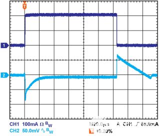
Figure 1. Transient response at COUT = 1 μF.
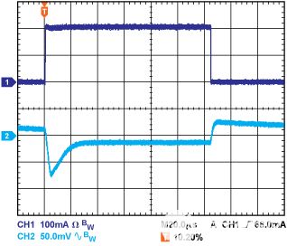
Figure 2. Transient response at COUT = 10 μF.
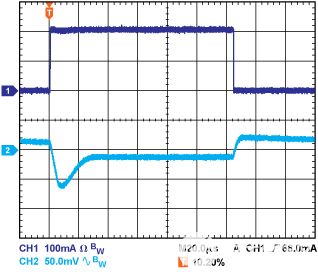
Figure 3. Transient response at COUT = 20 μF.
Input bypass capacitor
Connecting a 1 μF capacitor from V to ground reduces the sensitivity of the circuit to the printed circuit board (PCB) layout, especially when long input alignments or high source impedances are encountered. When more than 1 μF is required at the output, increase the input capacitance to match the output capacitance.
Input and output capacitor properties
Input and output capacitors must meet the minimum capacitance requirements for the expected operating temperature and operating voltage. Ceramic capacitors have a variety of dielectrics, each with a different behaviour relative to temperature and voltage. For 5V applications, X5R or X7R dielectrics rated from 6.3V to 10V are recommended. Y5V and Z5U dielectrics have poor characteristics with respect to temperature and DC bias and are therefore not suitable for use with LDOs.
Figure 4 shows the capacitance versus bias voltage characteristics of a 1µF, 10V X5R capacitor in an 0402 package. The package size and voltage rating of a capacitor have a significant impact on its voltage stability. In general, a larger package or higher voltage rating will provide better voltage stability. x5R dielectrics have a temperature variation of ±15% over the -40°C to +85°C temperature range, independent of package or voltage rating.
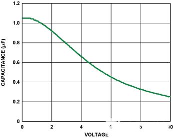
Figure 4. Capacitance versus voltage characteristics
To determine the worst-case capacitance over the range of temperature, component tolerance and voltage, adjust the nominal capacitance for temperature variations and tolerance as shown in Equation 1.
CEFF = CBIAS × (1 – TVAR) × (1 – TOL)
(1)
where CBIAS is the nominal capacitance at operating voltage; TVAR is the worst-case capacitance for temperature variation (as a fraction of 1); and TOL is the worst-case component tolerance (as a fraction of 1).
In this example, for the X5R dielectric, TVAR is 15% over the -40°C to +85°C range; TOL is 10%; and CBIAS is 0.94 μF at 1.8 V, as shown in Figure 4. Use these values in equation 1 to.
CEFF = 0.94 µF × (1 – 0.15) × (1 – 0.1) = 0.719 µF
The minimum output bypass capacitance of the ADP151 over the operating voltage and temperature range is 0.70 µF, so this capacitor satisfies this requirement.
Conclusion
To ensure the performance of an LDO, the effects of DC bias, temperature variations and bypass capacitance tolerances must be understood and evaluated. In applications where low noise, low drift or high signal integrity is required, capacitive techniques must also be considered. All capacitors are subject to non-ideal behaviour and therefore the capacitor technology chosen must match the requirements of the application.