In triode circuits, the direct current path and the AC path are often used to analyse the circuit, in effect using the circuit superposition theorem to analyse the circuit, which has two “sources”, a DC power supply and an input signal source.
The direct current path: the path through which the DC current flows under the action of the DC power supply, which is also the path through which the static current flows, is used to study the static operating point.
1) Capacitor is open circuit
2) Inductor coil is considered as short circuit
3) The signal source is considered as a short circuit, but retains its internal resistance

The first two are relatively well understood, with the capacitor isolated from DC and the inductor passing through DC. The third is the application of the superposition theorem, short-circuiting the signal source and analysing only the operating state of the circuit under the action of DC.
AC path: the path through which the AC signal flows under the action of the input signal, used to study dynamic parameters.
1) Capacitance with large capacity is considered as a short circuit
2) DC sources without internal resistance are considered as short circuits
The first one is as long as the capacitance is large enough and the input signal frequency is high enough, the capacitive resistance is negligible and the capacitance is considered as a short circuit. The second also uses the superposition theorem to short-circuit a DC source and only analyse the circuit operating state under the action of an AC signal source. Many people are confused by the DC short circuit analysis, in fact, the DC voltage source internal resistance is very small, when analyzing the signal source alone, the DC power supply can be considered a short circuit. It is really not good to understand, think of it this way, the DC voltage source has a lot of capacitance between the positive pole and GND, are through the AC.
The following input impedance is analysed in conjunction with the superposition theorem:
The dashed box on the left simulates a signal source with internal resistance R3= 5K and the output signal is connected to two voltage divider resistors.
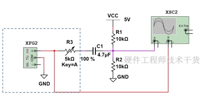
First look at the input and output waveforms.
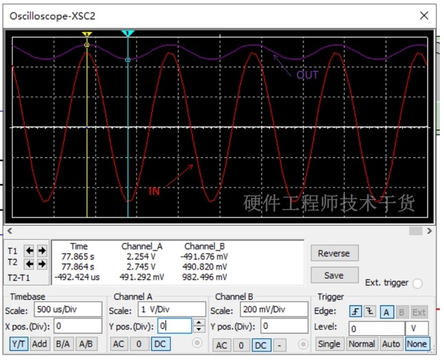
The red (Channel B) input waveform is a 1V peak-to-peak AC signal, while the purple (Channel B) output is a signal with a 2.5V DC component and a 500mV peak-to-peak value.
Why does this occur, we now use the superposition theorem to calculate.
1) Only DC VCC exists, DC cannot pass through C1, the output voltage is R1 and R2 divided, Uout1 is as follows
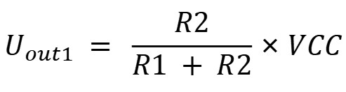
Substituting the corresponding values into the above equation gives Uout1 = 2.5V, which is equivalent to a DC bias. The presence of C1 makes this component independent of R3.
2) With only the AC signal source present and VCC connected to GND, C1 is equivalent to a short circuit for the AC signal and the output voltage is equivalent to R1 and R2 in parallel and then divided with R3, Uout2 is as follows
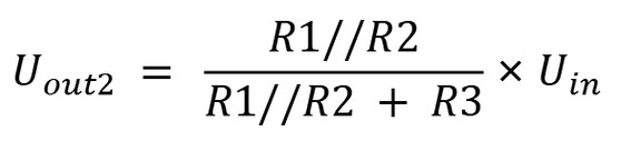
Substituting the corresponding values into the above formula gives Uout2 = 0.5Uin, Uin is a signal with a peak-to-peak value of 1V, so Uout2 is an AC signal with a peak-to-peak value of 500mV. According to the superposition theorem it follows that the output of these two signals when acting simultaneously is the sum of the two, i.e.
Uout = Uout1(dc) + Uout2(ac)
From the oscilloscope it is a signal with a 2.5V DC component and a peak-to-peak value of 500mV. The input AC signal is attenuated by half. This is caused by R3, which along with the back-end input resistor divides the input signal.
From here it is clear that if you do not want the input signal to be attenuated, you need to make R3 as small as possible and R1//R2 as large as possible, where the parallel value of R1 and R2 is the input impedance of the back-end network.
The so-called input impedance is for the input signal, i.e. the hindrance to the input signal, and has nothing to do with the DC bias. The input impedance is therefore R1//R2.
Turning to the common emitter amplifier circuit.
This circuit, described in the previous article, is a circuit with twice the amplification. The base current of the triode is so small that it can be ignored, or the in/out impedance of the triode is considered to be large and R2 in parallel is close to R2, so the input impedance of the common shot amplifier circuit is R1 and R2 in parallel.

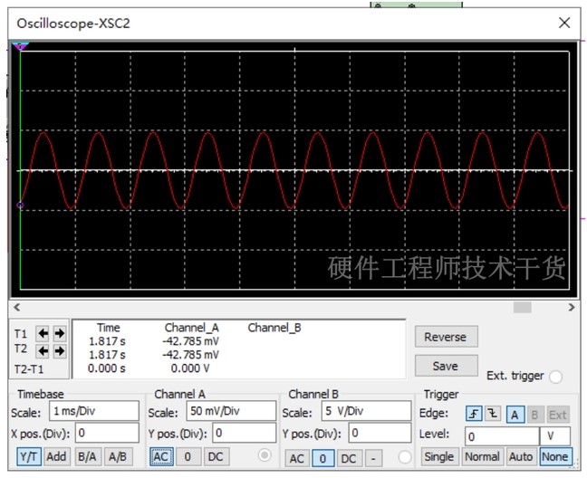
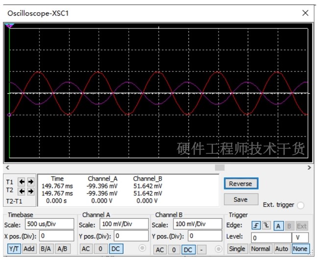
Now let’s verify this by adding an internal resistance R3 to the signal source, R3 = 17K ≈ R1//R2, with an input source of 1KHz and a peak-to-peak value of 200mV, and view the phenomenon.

The first measurement of the triode base waveform, found that the input signal was attenuated by half, into 100mV peak-to-peak value, which shows that the input impedance of the co-amplified circuit is R1 and R2 parallel value.
pYYBAGNstYmANb7LAAFaW2OhN90445.png
The input and output waveforms are in opposite phase and have the same amplitude, i.e. the amplification is 1 instead of the original 2 times. This is because the signal source is attenuated.

Output impedance.
Because the triode is a flow-controlled device, it can be seen as a constant-current source, except that the current of this constant-current source varies with the input signal. This constant current source is not very well understood, we combine simulation, say, the following figure in the input peak value of 200mV signal, measurement of each branch AC peak value as follows, here no matter how to adjust the load resistance RL, the collector current remains unchanged, and the sum of the load current and Rc current is equal to the collector current. It means that the collector current does not change with the load and the triode is equivalent to a constant current source.
The direct current path only provides a bias voltage, we can only analyse the AC path, the following is the AC path equivalent circuit.

We all know that the internal resistance of the constant voltage source can be seen as 0, the internal resistance of the constant current source can be seen as infinity, the emitter resistance Re can be neglected relative to the infinity resistance of the constant current source, so the output impedance of the common emitter amplifier circuit is Rc//∞, i.e., Rc. When adding a load resistor RL=Rc to the above circuit, the current flowing through Rc is halved because the current of the constant current source remains the same, resulting in the output the output voltage is halved.
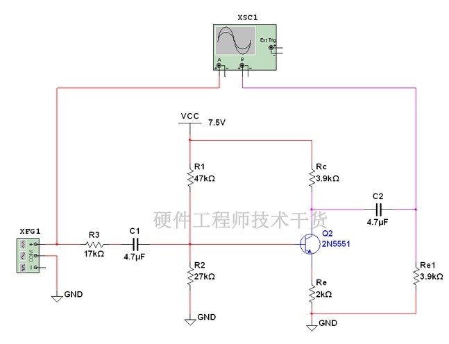
In the diagram above the input is 200mV peak to peak and the output is only 50mV, this is because the input signal is attenuated by half, the amplification is doubled and the output is again attenuated by half, so the output of this circuit is only 50mV peak to peak.