Today’s article explains all the important aspects of the rigid flex PCB. This article hopes to give large importers of the rigid flex PCB and OEM businesses an in-depth insight and analysis on sourcing PCBs.
We will cover areas such as the benefits, design guidelines, applications and more. At the end of this article, be sure of becoming an expert in this topic. Without wasting further time, let’s get started with what we have in stock for you.
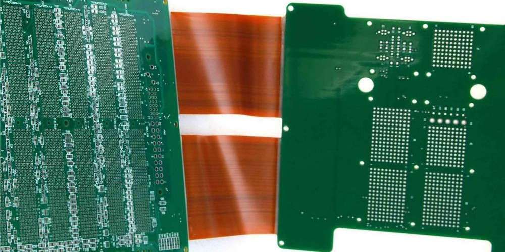
What are Rigid Flex PCBs?
Rigid-flex PCBs are those printed circuit boards that make use of a mix of rigid and flexible board technologies for a specific application. Majority of rigid flex circuit boards are made of many layers of circuit substrates that are flexible and are attached to at least one rigid board internally and/or externally depending on the application’s design. The designs of the flexible substrates are done to remain in the constant flex state and are during installation or manufacturing are made to form a flexed curve.
The designs of the Rigid Flex are usually more challenging in contrast to that of the rigid boards. This is because the design of these boards is done in a 3D space. This provides more spatial efficiency. With the ability to have a three dimensions design, the designers will be able to roll, fold, and twist the substrates of the flexible board in order to achieve the preferred shape.
What are the Types of the Rigid Flex PCB?
Rigid flex PCB comes in a few types. Let’s consider them
Single sided Rigid-Flex PCB
For the single sided type, they have just one conductive material layer. The board’s other side allows for the integration of different electronic components on your circuit board. Furthermore, they are made of a single layer of flex and rigid substrates combined together. In contrast to the other rigid flex PCB types, you can easily manufacture and design them.
Double Sided Rigid Flex PCB
For rigid flex printed circuit boards, they are composed of a single rigid substrate layer, while the other layer is a flexible substrate. This rigid layer aids in the enhancing of compactness. The flex substrate on the other hand plays a huge role in flexibility.
Furthermore, double sided rigid flex PCB permits more routing traces. The vias makes this possible, which alternates between both layers. Most PCB engineers prefer this type of rigid flex PCB due to the flexibility, as well as their capability to reduce the board size.
Multilayer Rigid-Flex PCB
This is a rigid flex PCB that features at least three conductive layers of any of both substrates. These substrates serve as insulators.
What are the Benefits of the Rigid Flex PCB?
Below are some of the major benefits of the rigid flex PCB
Lightweight and compact
Because rigid-flex PCBs are known to be flexible, they are lightweight as well. Furthermore, they are compact and this reduces the overall packing size. This is possible with the rigid substrate.
Flexibility
Flexibility is a characteristic of rigid flex printed circuit boards, which allows manufacturers to produce a board for existing devices. This contrasts producing a device when considering the specifications of the board.
Fits confined and smaller areas
The rigid flex PCB are very flexible, which makes them fit properly into smaller and confined areas. This leads to the miniaturization of the product. In essence, folding and bending it comes easily. This is what helps them fit into the small devices easily.
Reliable
Rigid flex PCBs are reliable because solder joints are absent. For the design, there are no connectors or solder joints in rigid flex PCBs. Also they lack contact crimps. With this feature, this PCB ensures integrity and reliability of applications that are manufactured using these boards.
Great thermal stability
When assembling the rigid flex PCB, the board utilizes polyimide. Polyimide has a great thermal stability, which helps it withstand harsh and extreme temperatures. This is why it is important in both defense and military applications.
Reduced Failure of the Circuit
The incorporation of both flex and rigid circuitry leads to the reduction of interconnections. By this, it helps in reducing circuit failure.
Cost Effective
The rigid-flex PCB is cost effective, as a result of the low requirement of the material. Rigid flex PCBs require fewer materials for their assembly. This leads to cost effectiveness since there’s a reduction in the cost of procurement as well as manufacturing.
THE ULTIMATE GUIDE TO XILINX FPGA, SERIES, AND ALL DETAILS
What are the Limitations of the Rigid Flex PCB?
We have discussed the benefits of the Rigid Flex PCB. Now, let’s know some of its limitations.
Requires Elaborate Manufacturing
When manufacturing the rigid flex printed circuit boards, you will need two substrates. These include the flex and the rigid substrates. Using both makes the production time-consuming and elaborate.
Labor intensive production
The rigid flex PCB production is not only material intensive, but also labor intensive. This is due to the sensitive nature of this PCB, as well as the variations that are inherent in the flex and rigid substrates.
The process of manufacturing is complex
Unlike the other simpler PCBs, the process of fabricating a rigid flex PCB is complex. It requires using suitable and effective software. All these make the production cost expensive.
What are the Guidelines for Rigid Flex PCB Design?
The PCB design and the layout stage is very important during the manufacturing process of the printed circuit board. Below are some of the main elements you should know.
Guidelines for Designing the Rigid Flex PCB
To design the rigid flex printed circuit boards, you must stick to the laid down rules. When making corners, ensure they’re not bent. If you have to make a bend, ensure that you have a curved bend in contrast to its being sharp.
Also, when changing the traces’ width, make sure that you do it gradually. Making abrupt changes can lead to a weak spot. Therefore to help in reducing costs as well as increase the flexibility of the circuit, you should use at least two flex layers.
Rigid Flex PCB Layout Guidelines
In order to create a rigid flex PCB successfully, there are some guidelines you need to observe.
Trace Width
Your calculator for trace width must deliver accurate results for the trace spacing and width between its flexible parts. Also, make sure that you complete the solder pads in either rounded or teardrop styles. This also applies to tracks.
Soldering Surface and Annular Rings
Also, it is important that you make sure that both the soldering surfaces and annular rings are large. You can achieve the thickness you desire using stiffeners.
However, the application of coverlays on flexible boards is important in rigid flex PCB. With this, you are giving the conductors some insulation and protection on its outer surface. When soldering, to restrain and hold the pads, the coverlay plays a very significant role.
Furthermore, the manufacturer has to make sure that the pads feature anchoring spurs. This ensures that there is no separation between the copper and the material during the assembly process.
Then, the pads should undergo fileting. This aids in reducing the stress points, as well as reduce the breakage chances when flexing.
Vias
You must metalize your plated vias. You can achieve this via the holes, which serves as a link between your flexible circuit and conductive layers.
The blind vias ought to connect its inner layer. You can also make use of the buried vias. Both help in connecting all the internal layers. However they ignore its outer layers. Making use of the different vias types will most probably augment any space that is present in the circuit. This allows different component pads to be added. The space is also useful for trace routing.
For rigid flex PCB’s flex circuits, it is important that you avoid using vias when working with the flex substrate. For cases where you must use this, areas where you will place them must not be bent.
You must also place some emphasis on the accuracy whenever you are calculating the rigid flex PCB’s bending radius. This ensures the absence of breakages.
What are the Steps in Designing the Rigid Flex PCB?
Below are the steps involved in the design of the rigid flex printed circuit boards.
Preparing the Base Material
Before you start the fabrication process, clean the laminate thoroughly. This is important since the use of the copper coils feature anti-tarnish features.
First, immerse the copper coil into an acidic solution. Also, you can spray the copper coils with acid, if this is preferable. After, you micro-etch the coils. To make this happen, use sodium persulphate in treating the copper coil.
Third, is coating the coil in a comprehensive manner. You achieve this by making use of different oxidation agents.
Generating the Circuit Pattern
Here you will be creating the circuit pattern. Here, you will be using two major techniques, which are photo imaging and screen printing.
Photo Imaging: This technique, those the oldest, is still a frequently used method. This technique makes sure that the dry photoresist film rests on the laminate. You then expose the material to ultraviolet light. Furthermore, you can transfer the photomask pattern to the laminate.
Screen Printing: This is a preferable method because it can produce the right circuit patterns. This is possible because it can deposit on the surface of the laminate accurately.
Circuit Pattern Etching
Rigid flex PCB manufacturers make this happen when you dip the laminate inside an etch bath. Another method you can use is to spray them making use of the right etchant solution. To get the necessary results, you can do etching on the two sides simultaneously.
Drilling
For drilling, the vias, pads, and holes are drilled. In order to have precise holes, make sure that your drilling tools have the ability to sustain a high speed. Make use of the methods of laser drilling when creating ultra-small holes.
Through-hole Plating
You must handle this step with much precision and care. After drilling the desired hole, you deposit copper into them. By doing this, they are chemically plated. Finally the result is forming of the electrical interconnections through the layers.
Applying the Covercoat or Cover Lay
Next is to apply the Covercoat or cover lay. This is to help you protect the flex circuit’s top and bottom sides. This protection is from all hostile environments including solvents and harsh chemicals.
Cutting Each Flex
This has to do with cutting each of the flex boards from that panel where you are conducting the production. This is a very important step during the production of rigid flex. You must do this with precision and care.
Electrical Testing
The final test is to conduct several tests on the board. This includes circuit performance as well as the quality making use of the specifications of the design as a threshold.
How to Choose the Best Rigid Flex PCB Manufacturer
Expertise and Experience
Work with manufacturers that are experts in the process of fabrication. Their experience as well will guarantee quality products
Manufacturing Capability
There are manufacturers that cannot handle mass production. This is because they lack cutting-edge facilities for production. Therefore work with companies that can meet your desires.
Technical Support
The manufacturer must have a staff with great qualifications and experience. Also, this is important to make sure that the product meets the needed standards.
Cost
Before you work with any manufacturer, make sure that you do your research regarding market prices. With this, you will be able to negotiate prices better when dealing with that manufacturer.
What are the Applications of the Rigid Flex PCB?
The applications of the Rigid Flex PCB include:
- Aerospace Industry
- Military equipment
- Medical Industry
- Automotive Industry
- Telecommunication Industry
- Consumer Appliances
Conclusion
The rigid flex circuits are complex board types. This is because they combine the rigid and flex substrates. Furthermore, the applications that are generated from these printed circuit boards are very important to the users’ well-being.
Make sure that you work with the necessary procedures and guidelines we have written in this article. This helps in ensuring that whatever applications are generated from these boards meet the necessary standards and are safe.