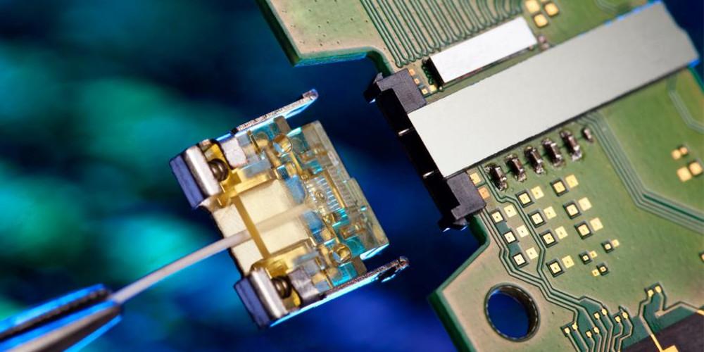
Integrated circuits are chips having electronic components, which forms an effective and functional circuit. These include those that are embedded in smartphones, computers, as well as other different electronic devices. The photonic circuits, on the other hand, are any chip containing photonic components. These are those components working with photons or light.
For electronic chips, the electronic flux is usually passed through different electrical components. These include inductors, resistors, capacitors, and transistors. Furthermore, in photonic chips, the photons usually pass via optical components like waveguides (these are just like the electrical wires or resistors), lasers (which are just like transistors), phase shifter and polarizers.
How Does a Photonic Circuits Work and What Problems Can it Solve?
The photonic circuits make use of a laser source in injecting light, which helps in driving all the components. This is just like turning a switch on to help in injecting electricity that helps in driving the electronic components.
Making use of light rather than the use of electricity, the photonic circuits technology offers a reliable solution to all the possible limitations that electronics pose. These include heat generation and integration, taking the devices to a higher level, to help in increasing the speed and capacity of data transmission.
Furthermore, the photonic circuits offer benefits like higher speed, miniaturization, large integration capacity, low thermal effects, as well as compatibility with the already existing processing flows, which permits lower prices, volume manufacturing, and high yield. The applications serving integrated photonics are usually broad. This is from data sensing and communications to automotives as well as astronomy.
Applications of the Photonic Circuits
Data communications is a very important application field for the photonic circuits. Sensing follows (which is for autonomous driving and agriculture), as well as biomedical applications like lab on a chip devices and applications that serve in the aerospace and defense industry, and the astronomical field
The additional applications and improvements for the photonic circuits keeps emerging as different designers face technological challenges in areas whereby the integrated photonics could play an important role as well as areas whereby feasibility studies could help in determining if it promises a solution.
These photonic circuits can help in finding applications in many different areas. Here are some of them:
- Optical fiber and free space communications can make use of circuits for the regeneration, detection, and generation of signal as well as other forms of processing.
- Also, it is applicable in optical metrology. For example, it takes the form of fiber-optic and LIDAR sensors, which can benefit from photonic circuits. This can happen even where delicate devices like interferometers can happen in a stable and compact manner.
- Furthermore, with optical frequency metrology, you will be able to make use of very compact frequency sources like the optical frequency synthesizers.
- Another application of photonic circuits is the Terahertz imaging. This usually deals with the photonic elements that aids in the generation and detection of terahertz waves as well as processing of the signals.
- Also, quantum computing and quantum cryptography is another application of photonic circuits.
Frequently, the photonic circuits are fabricated and designed specifically for different and unique applications. You can refer to them as ASPIC. This means the application of specific and photonic integrated circuit or photonic circuits.
What are the Benefits of Developing Photonic Circuits?
With the electronic integrated circuit, now coming up close to the end of the integration capacity, the photonic circuits have the ability to become the most acceptable technology serving
- Data communication These include intra- and inter-datacenter communications
- Sensing for aeronautic and aerospace
- LiDAR solutions that aid autonomous driving
- Untold applications for the future in the new ear for technology.
What are the Basic Steps in Developing Photonic Circuits?
The process involving the appropriate design and photonic circuits could be complex. The steps involved usually vary. This depends on the foundry and the application. The steps include:
- Identifying your requirement or idea
- Performing your application’s feasibility study
- The design (this considers the packaging and PIC testing from the start and beginning
Level of the device (these includes the material, thermal, and optical simulations)
The Circuit level (this is the virtual lab that helps to test the performance)
The System level (The photonic circuits connected to the communications links)
Layout level (This generates your design intent)
Verification (LVS and DRC for high-yield assurance and manufacturing compliance)
GDS (Take a look at the generated mask, then replace the white/black boxes where necessary)
- The process flow
Simulation of all the process steps
- Fabrication
- The testing
Wafer level
The chip level
- Packaging
Fabrication in the Foundries

In the microelectronics industry, the foundries model is widely accepted. This indicates a separation present between a specific company involved in the designing as well as later selling the integrated circuit to serve a purpose and then another company which is known as the foundry for the fabrication.
The foundry alone has to possess the detailed know-how and complex machinery necessary for fabrication. This same model also works for the photonic integrated circuit. Once again, you will need a complex technology that is mastered properly by some of the foundries, and therefore, some of their customers will be able to focus on the designing of the circuits to deliver some specific purposes and also bring them to the market
Furthermore, you need to develop a reliable and suitable interface whereby the foundry will describe the capabilities as well as receive the design you need to fabricate. Also, for the designs, you may have already predefined some elements, and you may connect them appropriately using the circuits designer. These elements are useful for realizing some design functions such as modulators, resonators, couplers, waveguides, photodetectors, etc. Lastly, this foundry may help in fabricating the bare chips and can offer some packaging solutions.
Conclusion
Photonic circuits come with lots of benefits. To summarize, the photonic circuits, on the other hand, are any chip containing photonic components. These are those components working with photons or light.