Keypad driver based on N32G45
1.N32G45 Introduction
The N32G45 series integrates the latest generation of embedded ARM Cortex™-M4F processor with enhanced computing power, new floating point processing unit (FPU), DSP and parallel computing instructions based on the Cortex™-M3 core, providing excellent performance of 1.25DMIPS/MHz.
The combination of efficient signal processing capabilities and the low power consumption, low cost and ease of use of the Cortex-M family of processors is designed to meet the needs of easy-to-use applications requiring a mix of control and signal processing capabilities.
The ARM Cortex™-M4F 32-bit lean instruction set processor offers excellent code efficiency, and the high performance of the ARM core can be achieved with the memory space typically available in 8-bit and 16-bit devices.
- N32 Peripheral Features
Up to 512KByte on-chip Flash with encrypted storage, multi-user partition management and data protection, hardware ECC checksum, 100,000 erasures and 10 years data retention.
144KByte on-chip SRAM (including 16KByte Retention RAM), Retention RAM supports hardware parity check.
Communication Interface
- 7 U(S)ART interfaces, up to 4.5 Mbps, including 3 USART interfaces (supports 1xISO7816, 1xIrDA, LIN), 4 UART interfaces – 3 SPI interfaces with speeds up to 36 MHz, 2 of which support I2S – 1 QSPI interface at up to 144 Mbps – 4 I2C interfaces at up to 1 MHz, master-slave configurable, dual address response support in slave mode – 1 USB2.0 Full speed Device interface – 2 CAN 2.0A/B bus interfaces – 1 SDIO interface, SD/MMC format support

ADC analog interface
-2 12bit 5Msps high-speed ADCs with configurable accuracy, up to 9Msps sampling rate in 6bit mode, up to 18 external single-ended input channels, differential mode support
-2 12bit DACs with 1Msps sampling rate
–External input independent reference voltage source support
–All analog interfaces support 1.8~3.6V full voltage operation
Supports up to 97 GPIOs with multiplexing capability, most GPIOs support 5V withstand voltage.
2 high-speed DMA controllers, each supporting 8 channels, with arbitrary channel source and destination addresses
RTC real time clock, leap year calendar, alarm events, periodic wake-up, internal and external clock calibration support
Timing counter
–2 16bit advanced timer counters, support input capture, output comparison, PWM output and quadrature encoding input, etc. Maximum control accuracy 6.9nS. 4 independent channels for each timer, 3 of which support 6 complementary PWM outputs
— 4 16bit general-purpose timer counters, each with 4 independent channels, supporting input capture/output comparison/PWM output
—2 16bit basic timer counters
-1x 24bit SysTick
-1x 7bit Window Watchdog (WWDG)
-1x 12bit Independent Watchdog (IWDG)

3.N32G457VEL7 based development board introduction
N32G45XVL-STB development board is used for the prototype development of high performance 32-bit N32G45XVL series chip of National Technology Co. Based on ARM architecture Cortex-M4F core, clock frequency is 144MHZ, storage space flash size is 512KB, run space Sram size is 144KB.
Support serial download, Jlink download emulation, USB download and CMSIS-DAP download emulation. The board itself comes with CMSIS-DAP interface circuit.
The schematic of the development board is as follows

- Key operation based on N32G45
The project creation of N32G45 can be seen in the post: https://bbs.elecfans.com/jishu_2320004_1_1.html
- To implement the key driver can be divided into three steps: 1. open the clock; 2. configure the GPIO port; 3. pull up and down.
Next, we first look at the hardware interface of the keypad, the schematic diagram is as follows.
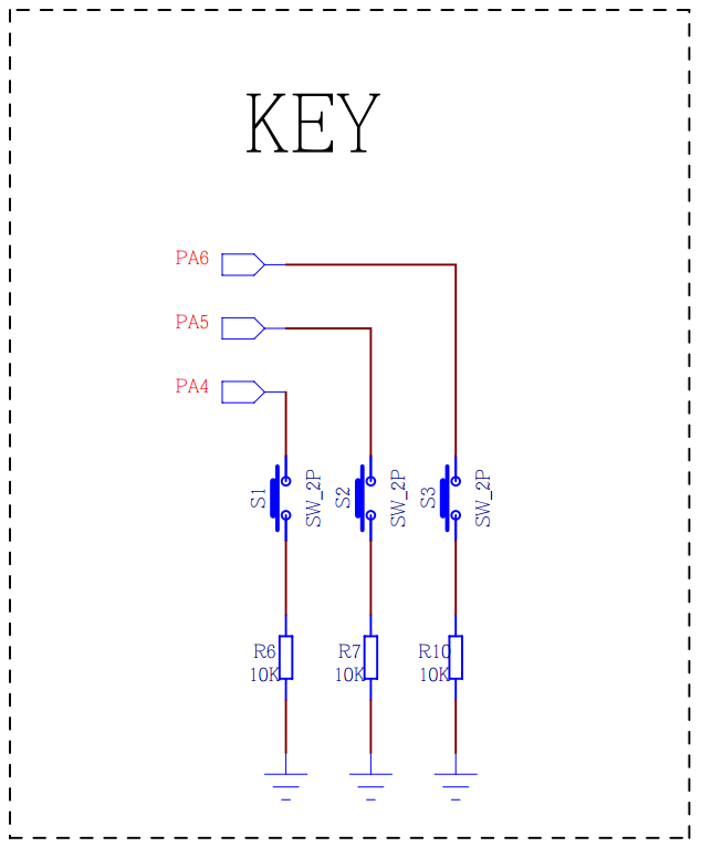
According to the schematic diagram, the hardware interfaces for the keys are
S1 —PA4 S2 —PA5 S3 —PA6
With the hardware interface, we can just follow the 3 steps.
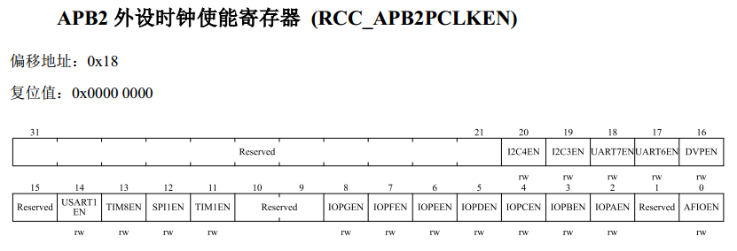
Turn on the clock
To turn on the clock, we can first look at the system architecture of the N32G45, the system architecture block diagram is as follows.

According to the system architecture block diagram, we can see that the whole kernel structure is divided into three buses: AHB, APB2, APB1. where the AHB bus clock frequency is 144MHZ, the clock bus on APB2 is 72MHZ, and the clock bus on APB1 is 36MHZ.
According to the key schematic, we only need to turn on the PA clock
Configuring the GPIO port
For GPIO port configuration, we need to refer to chapter 7 of the user manual.
The chip supports up to 97 GPIOs, which are divided into 7 groups (GPIOA/GPIOB/GPIOC/GPIOD/GPIOE/GPIOF/GPIOG) with 16 ports in each group (10 in group F and 7 in group G). . The GPIO ports share pins with other multiplexed peripherals and can be configured flexibly according to user requirements.
Each GPIO pin can be independently configured as an output, input, or multiplexed peripheral function port. All GPIO pins, except the analog function pins, have high current pass-through capability.
The GPIO ports can be configured separately by software in the following modes.
■ Input float
▪ Input pull-up
■ Input pull-down
■ Analog function
■ Open-drain output
■ Push-pull output
Push-pull multiplexing function
Open-drain multiplexing function
Corresponding to the keys, we need to configure the mode for push-pull output.
Port mode configuration register.

The key GPIO port is configured as follows.
/* Configure the GPIO port*/
GPIOA->PL_CFG&=0xF000FFFF;
GPIOA->PL_CFG|=0x08880000;// pull-up/pull-down input mode
Note: Since the key is doing detection to determine whether the key is pressed or not, the key mode configuration needs to be set to input mode.
Pull Up/Down
The pull-up/pull-down operation, i.e. setting the initialized level state. It can be implemented by GPIO_POD or GPIO_PBSC.
According to the key hardware schematic, the key press is low level, to detect whether the key is pressed properly, it needs to generate a jump process from high level to low level, so the key needs to be set to pull-up mode.

3.2 Keystroke detection
To facilitate the subsequent use of keys, we can wrap a separate key detection function to determine which key is pressed by the return value.
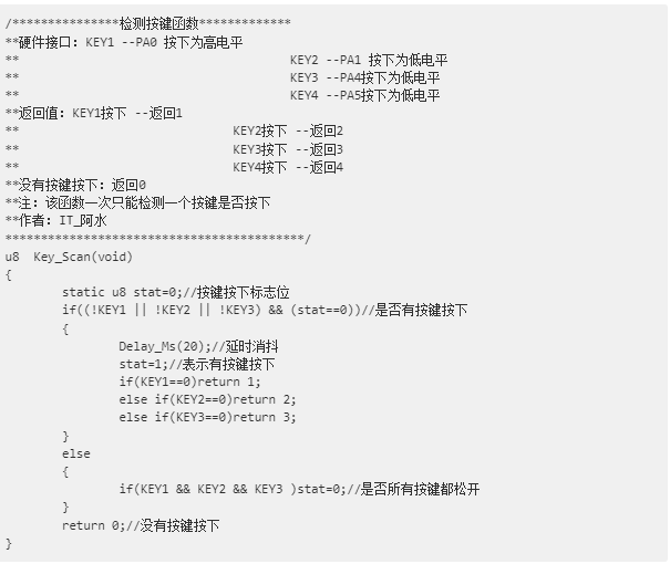
Note that the above functions KEY1, KEY2, KEY3 are achieved by bit with the way, the specific writing method to view the post: https://bbs.elecfans.com/jishu_2320004_1_1.html
3.3 Keystroke Control LEDs
The LEDs are controlled by any one of the keys.
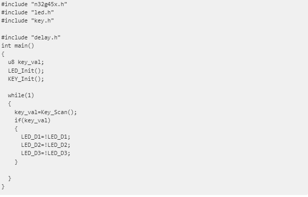
The achieved effect is as follows.
Press the button and all the LEDs light up, press the button again and all the LEDs go off.