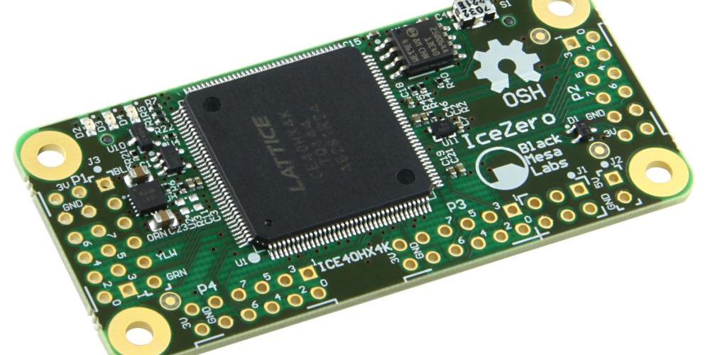
iCE40 FPGA is a low-power and high-performance Field Programmable Gate Array (FPGA). Manufactured by Lattice Semiconductor, it offers a combined function of low-power and high-performance – all from a compact BGA FPGA package.
if you want to know what makes iCE40 FPGA one of the reliable FPGAs you can work with, read this article to the end.
Understanding the Low-Power Basis
It is worthy of note here that the low-power basis of the iCE40 FPGA takes a cue from the generalist approach of the manufacturer to producing FPGAs that use the least power. Wikipedia noted that the iCE40 FPGA is one of the numerous low-power FPGAs broadly categorized under iCE40.
Least Power Usage
The manufacturer hinted that the iCE40 FPGA, like the other iCE FPGAs, was built “from the ground up for low power starting at 25 µW.”
Thus, you can count on iCE40 FPGA to minimize or reduce power consumption, while maximizing the available battery life.
Target Applications
iCE40 FPGA is designed for use with the ultra-low power and the always-on applications. The FPGA can also be used with the portable and battery-powered devices.
Why the Low-Power Optimization?
Lattice Semiconductor purposely optimized iCE40 FPGA for the low-power applications for several reasons. The major reason is because of the manufacturer’s commitment to making programmable devices that can help offload some power-centric loads from the System-on-a-Chip (SoC) or the target device’s core processor.
How iCE40 FPGA Improves Battery Life
Just as it reduces power usage, iCE40 FPGA also expunges on the battery life. The batter life is improved because of the potential of the peripherals and the main (core) processor to enter the low-power state. The aforementioned can also be entirely powered off. Either way, it paves the way for iCE40 FPGA to cut down on power usage and extend the device’s battery life.
Features of the iCE40 FPGA
Below are some of the additional features that make iCE40 FPGA outstanding:
1. Compact Size
iCE40 FPGA is a compact or space-saving FPGA. Despite the architectural demands, it can comfortably fit into the “most space-constrained modules.”
Worthy of mentioning is that the iCE40 FPGA has a broad range of 0.35mm and 0.40mm of the pitch BGA package.
2. Image Sensor Sourcing
The image sensors are multi-sourced, as that feature was enabled via the implementation of flexible bridges that support the common interfaces. Examples of the supported interfaces are:
- Parallel LVCMOS
- HiSPI
- LVDS and;
- subLVDS
3. The Tri-Series
It is true that the iCE40 FPGA is a low-power and apace-saving FPGA. One other attribute is that it is readily available in three (3) series.
These include:
- HX: this refers to the high-performance variant of iCE40 FPGA
- LP: this is the core or primary iCE40 FPGA, which offer lower power usage
4. Display Matching
You can now match your preferred display to the target application via the following supported interfaces:
- MIPI DPI/DBI
- RGB
- 7:1 LVDS
5. Flexible Device Configuration
A couple of factors are responsible for the configuration of the target devices supported by iCE40 FPGA. It has to do with the FPGA’s support for the SPI Cores and the Integrated Hard I2C.
Those integrations pave the way for flexible device configuration via the SPI interface.
Technical Design of the iCE40 FPGA

The technical stackup of this Field Programmable Gate Array (FPGA) integrates a wide range of features and components.
Below are some of the components making up iCE40 FPGA’s architecture:
The PLBs
This refers to the Programmable Logic Blocks, that is, blocks that can be reprogrammed to fir into the respective uses.
iCE40 FPGA supports eight (8) logic cells per block. The logic cells, on the other hand, have the following general compositions:
- D flip-flop (this is where the output of the Lookup Table is connected).
- Four-input Lookup Table (LUT)
I/O Pins
The Input and Output (I/O) pins on iCE40 FPGA are further separated into four (4) banks. These are then used to facilitate the low-power and battery life maximization.
For example, separate power-supply pins can be attached to each of the banks, depending on the targeted devices. If that is the case, the integrated power-supply pins can be used as a tool to enable the logic-high voltage level of the I/O banks to be adjusted.
Furthermore, the configurability of the I/O’s voltage levels allow for the support of several interface standards, whereby the voltage levels range between 1.8 volts and 3.3 volts.
Data Storage Capabilities
iCE40 FPGA, like the other iCE FPGAs, uses the volatile SRAM memory to store configuration data. That way, the configuration data must be loaded into the target device anytime there is power outage.
While that is the primary means for storing configuration data, the options can also be stretched a bit. The following are the additional options for loading the configuration data into the target devices:
- Chip
- Programmer
- An external flash memory chip
Variations of the iCE40 FPGA
You can make your choice of the iCE40 FPGA from the core provisions. Optionally, you can pick from any of the supported variants. The following are some of the related FPGAs:
iCE40 LP/HX FPGA
This is the iCE40 FPGA that combines low-power with high-performance. It does that to enable the power-savings on the target devices, while making those devices fully-functional.
The iCE40 LP/HX FPGA features the following:
- Space-Free Constraints: this FPGA removes most of the barriers or design challenges that could have hampered both customization and innovative design. This is enabled via the ultra-small 1.4mm x 1.4mm x 0.45 mm WLCSP package.
- Design Tools: iCE40 L/HX FPGA offers a wide range of design tools to help you kickstart the designs. The list of supported tools includes reference designs, and demos.
- Flexible Architecture: the logic architecture is flexible because of the 3,520 4-input Lookup Tables (LUTs). The FPGA also supports up to 26 Input and Output (I/O) pins that enable customization of the interfaces.
iCE40 UltraPlus & UltraLite FPGA
This is the iCE40 FPGA variant that combines Machine Learning (ML) and Artificial Intelligence (AI) for the performance.
The features include:
- The implementation of Neural Networks for “pattern matching necessary to bring always-on intelligence to the edge.”
- The use of DSP blocks to enable high-performance signal processing.
- Provision of low-power computational resources “for higher levels of intelligence.”
Wrapping Up
The iCE40 FPGA is an ideal FPGA for use with low-power-centric applications and which require maximum performance. You can either choose between the iCE40 LP/HX FPGA that combines low-power and high-performance or the iCE40 UltraPlus and UltraLite FPGA variant that integrates Machine Learning (ML) and Artificial Intelligence (AI) for introducing “edge intelligence to FPGAs.”