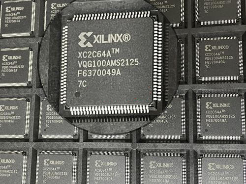
Core3S500E is a core development board for Field Programmable Gate Arrays (FPGAs). The board features the Xilinx XC3S500E, an FPGA built on the Xilinx Spartan-E series. In this article, you are going to discover some of the ways the board supports the expansion of FPGAs.
Importance of Core3S500E
Core3S500E is an FPGA core development board, optimized to provide a robust hardware for the design and optimization of Field Programmable Gate Arrays (FPGAs).
The board is well-equipped with the single-chip solutions and relevant hardware fabric for creating ultimate design flexibility for programmable devices. If you are looking to work with the Core3S500E, here are some of the additional things you need to know about it.
FPGA Expansion

Core3S500E features the XC3S500E, an FPGA by Xilinx. It helps to further expand this device in terms of the additional components added to it.
Core3S500E Properties
These are some of the properties making up the mechanics of the Core3S500E FPGA core board.
1. Configurability
The board is easy to programme and features a JTAG interface for the debugging and programming of the relevant interfaces.
The Core3S500E’s configured data is then downloaded to the standard JTAG interface or any of the following:
- FPGA Active
- FPGA Passive
2. Power Supply Circuit
The core board relies on the PWR LED for checking the (power) operation status of the Core3S500E. It does it via the connection to the 3.3-volt output.
On the other hand, the Core3S500E core board is able to function optimally by getting adequate power supply. This is achieved via the conversion of the 5-volt input voltage to fragments of 1.2-volt, 2.5-volt and 3.2-volt.
Voltage standards are also maintained adequately via the connection of the VCCO_0/1/2/3 IO voltage to either of the:
- 1.2-volt
- 1.5-volt
- 1.8-volt
- 2.5-volt
- 3.3-volt
3. Core Board Extension

Extending the performance of the Core3S500E is one of its core attributes. It has to do with the extendable interface of the board that allows for the optimization of the board as per the compatible to other FPGA boards.
The extensibility of the Core3S500E’s design circuit also allows the users to optimize it as per the needs or the targeted applications’ specifications.
4. Reset Circuit
Want to start all over again or make a general change to the Core3S500E FPGA core board’s design? The reset circuit helps you do that.
The primary role of the reset circuit is to reconfigure the Field Programmable Gate Array (FPGA) without having to reboot the device.
5. Data Retention
Retaining the data in an FPGA even without any power supply is one of the features you want to check out on the Core3S500E.
It achieves that by using the PROM XCF04SA, which is a Platform Flash series of the in-system programmable configuration PROM.
By connecting to the PROM, Core3S500E is now able to retain or store the configured data, even when the board isn’t powered.
6. Excellent Clocking
Core3S500E uses the GCLK, a dedicated global clock input that drives the main clock, as well as controls the timing of each of the devices.
Final Words
The Core3S500E FPGA core board makes configuring the Xilinx XC3S500E worthwhile, while providing the platform and peripherals neede
