According to the link in the inspection process, IC IC inspection is divided into design verification, front channel measurement and inspection, and back channel inspection. Optical measurement is performed indirectly by analyzing the reflection and diffraction spectra of light, which has the advantages of high speed, high resolution and non-destructive. The back-end inspection process is the “quality inspector” of the chip production line. According to the sequence of the process in the packaging process, the back-end inspection can be divided into CP test and FT test.
In the above tests, the spectrometer can be used in processes such as film thickness measurement and etch endpoint monitoring.
1.Film thickness measurement
The production of semiconductor integrated circuits is based on tens to hundreds of times of coating, lithography, etching, de-coating, and flattening as the main processes. The thickness and uniformity of the film layer directly affects the quality and yield of the chip, and the thickness of the film layer must be constantly inspected and controlled during processing. Optical thin film thickness gauge is one of the essential equipment in the semiconductor production process, used to test the coating thickness of chip wafers and related semiconductor materials, etc.

The two main types of semiconductor optical thin film thickness gauge technology are spectral reflectometry and ellipsometry. Ellipsometer takes into account the polarization of light, uses the phase difference between P-wave and S-polarized reflected light, is suitable for very thin films, and can directly test N,K values. The spectral reflectometer does not have these properties of the ellipsometer, but it can also measure the thickness of films below several nanometers with high measurement accuracy and faster measurement speed.
Based on the interference phenomenon of light waves, the light beam is irradiated on the surface of the film, and the incident medium, film material and substrate material have different values of refractive index and extinction coefficient, which makes the light beam reflect on the upper and lower surfaces of the transparent/semi-transparent film, and the reflected light waves interfere with each other, thus forming interference light, and the intensity of these interference lights at different phases will change with the thickness of the film. The thickness of the film can be calculated by detecting the interference light and combining it with an appropriate optical model.
Ocean Insight film thickness gauge inspection system, equipped with sampling platform, UV-VIS reflection probe, the configuration is as follows.
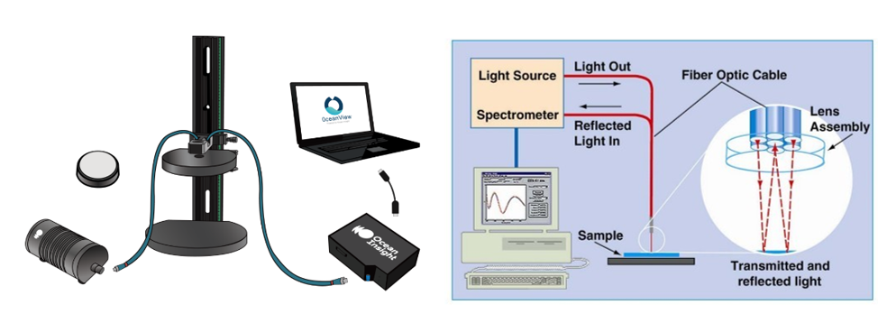
Figure 1: Film thickness measurement system configuration
Endpoint Monitoring
In a plasma-based etch process, plasma monitoring is important for process control. Wafers are fabricated and manipulated using photolithography, and etching is a major part of the process where the material can be layered to a very specific thickness. As these layers are etched on the wafer surface, plasma monitoring is used to track the etching of the wafer layers and to determine when the plasma has completely etched a specific layer and reached the next layer. By monitoring the emission lines generated by the plasma during the etching process, the etching process can be accurately tracked. This endpoint detection is critical for the production of semiconductor materials using plasma-based etching processes.
Plasma monitoring can be accomplished with a flexible, modular setup using a high-resolution spectrometer such as Ocean Optics’ HR or Maya2000 Pro series (the latter is a good choice for UV gas detection). For modular setups, the HR spectrometer can be combined with an anti-exposure fiber to obtain qualitative emission data formed in the plasma. Qualitative emission data is obtained from the plasma formed in the plasma chamber. If quantitative measurements are required, the user can add a library of spectra to compare data and quickly identify unknown emission lines, peaks and bands.
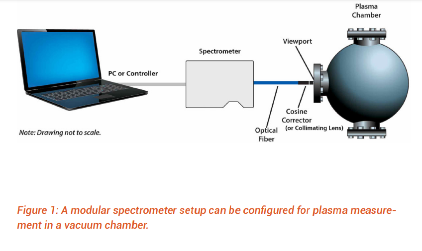
Figure 2: The modular spectrometer setup can be configured for plasma measurements in a vacuum chamber.
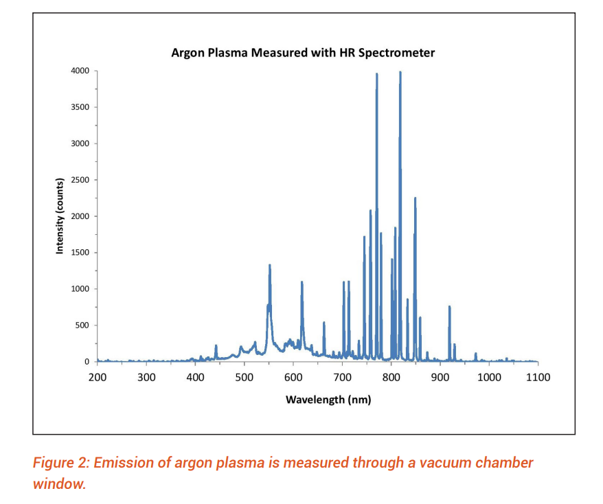
Figure 3: Measurement of argon plasma emission through the vacuum chamber window.
UV-Vis-NIR spectroscopy is a powerful method for measuring plasma emission for elemental analysis and precise control of plasma-based processes. These data illustrate the capability of modular spectroscopy for plasma monitoring. the Maya2000 Pro has a very good response in the UV. In addition, the spectrometer and subsystems can be integrated into other devices and combined with machine learning tools to enable more sophisticated control of plasma chamber conditions.
Spectroscopic applications in the semiconductor field are one of Ocean Optics’ future business focuses. The name change from Ocean OpTIcs to Ocean Insight is also the beginning of Ocean Optics’ strategic realignment from a spectroscopy product manufacturer to a spectroscopy solution provider. Ocean Optics not only continues to enrich and expand its optical sensing product line, but also enhances its support and service capabilities to provide customized and systematic solutions and application guidance to customers who need customized solutions. As an official authorized partner of Ocean Optics, iFrog Technology is committed to working with Ocean Optics to help customers face problems, explore future issues, and create customized spectroscopy solutions.