Data merging converter based on EPM7128 design
When a data switch has a high transmission rate, it sends data to the serial port in two parts before sending, and then the data from each serial port is merged together and converted into a PCM stream by a data merging converter. This paper introduces the data merging converter designed based on CPLD chip EPM7128.
1 Data merge converter hardware circuit
EPM7128 is a programmable large-scale logic device, ALTERA’s MAX7000 series, with high impedance, electrically erasable and other characteristics, available gate cells for 2500, the maximum delay between pins is 5ns, the operating voltage is +5V.

The IDT7205 is a FIFO type asynchronous read/write memory chip with a capacity of 8192 x 9 bits, access time of 12ns, three flag bits of empty, half full and full, maximum power consumption of 660mW and operating voltage of +5V.
MSM4860DX belongs to the PC104 embedded system of 5X86 series tenth, for AMD-133MHz CPU, with COM1, COM2 two serial ports, a LPT parallel port, an ELOPPY interface, an IDE interface, a VGA/LCD interface, an AT-KEYBOARD interface, 16 interrupts, rated at 8W. The operating voltage is +5V.
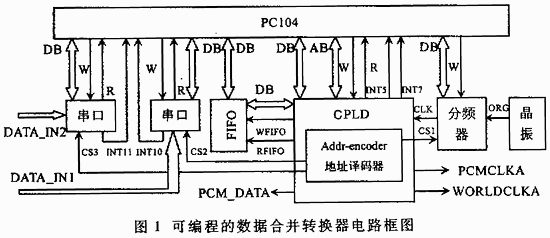
1.2 Block diagram of data merging converter circuit 2.2 Data shifting part Let the frequency of PCMCLK be f(MHz), then the frequency of FRAMECLK is f/8. Since the frame length is 64, we have: frame frequency=f/(8×64),PCM stream rate=f(bit/s). The frequency division ratio of the divider is set by software, so the rate of the PCM stream is programmable.
The block diagram of the programmable data merge converter circuit is shown in Figure 1. In the figure, DB is the data bus, AB is the address bus, R and W are the read/write signal lines, INT5, INT7, INT10 and INT11 are the four interrupts, CS1, CS2 and CS3 are the address decoder Addr-encoder generated inside the CPLD to send to the divider and the two serial port chip select signals respectively, ORG is the crystal oscillator to send to the divider The CLK is the pulse FRAMECLK and PCMCLK output from the divider, WFIFO and RFIFO are the read/write pulses generated by CPLD to access the FIFO containing address information, DATA_IN1 and DATA_IN2 are the serial port input data, PCM_DATA is the PCM stream output from the data merge converter, PCMCLKA is the output PCMCLKA is the output code synchronization clock and WORLDCLKA is the output word synchronization clock.
1.3 Circuit Operation Analysis
The crystal sends the clock pulse to the divider, which contains two programmable timers. The divider sends the controllable FRAMECLK and PCMCLK to CPLD, which forms three pulse signals inside CPLD after logic combination, one way to control the counter to form INT5, INT7 two frame frequency interrupt trigger pulses, the CPU receives the interrupt to write FIFO immediately; the other way to control the shift register to convert parallel data into serial data PCM stream; the third way to form Two serial ports through the interrupt mode (INT10, INT11) received external data, temporary storage buffer, according to a certain format by the interrupt INT5 control write to the FIFO.
2 CPLD internal logic circuits
2.1 Address decoder
Addr-encoder is generated in VHDL. The outputs of Addr-encoder are bus driver chip 74245 enable pulse ENB, bus transfer direction enable pulse DIR, write FIFO operation pulse WFIFO, divider and serial port chip select CS1, CS2 and CS3, FIFO data empty full flag pulse RFIFOFLAG, FIFO reset clock pulse WCTRL.

FRAMECLK period is 8 bits of PCMCLK, and they are both pulses sent by dividing the frequency. FRAMECLK is inverted as the read signal of FIFO, and twice inverted as the word synchronous clock. PCMCLK is directly used as the clock trigger pulse of shift register 74165, and the output low level after both with and without is used as the trigger level of 74165 re-data. Their signal timings are shown in Figure 3.
From the timing diagram of the three, it can be seen that whenever the last bit of a byte finishes shifting, the FIFO data is read under the falling edge of the FRAMECLK pulse inversion trigger, when the 74165 loading enable 74165STD happens to be low (with or without the result), completing the data loading of the part, and then a new soft time of data shifting starts under the rising edge of the PCMCLK pulse.
2.3 Part of the frame length counter
Two 74161 design long 1/64 divider, also called frame length counter, the clock of this counter is FRAMECLK, the counter output the highest two logic with for interrupt INT7, put with the gate output with the next higher logic iso-or for interrupt INT5. so that INT7 than INT5 in the timing of half a cycle earlier. After the start of reset, INT7 pulse is generated first, triggering the interrupt, COU interrupt after the service program to write 64 bytes of data to the FIFO, and then mask interrupt INT7, half a cycle later, there are 32 bytes of data left in the FIFO (so the FIFO read pulse and FRAMECLK inverse the same frequency). Then interrupt INT5 comes, the CPU responds, and then write 64 bytes of data to the FIFO, so that the FIFO has been maintained in the state of data (can avoid reading the FIFO falls exactly between the two write FIFO, the FIFO due to no data and read dead). In this way, whenever interrupt INT5 comes, 64 bytes are written to the FIFO, week after week, so 64 bytes are set as the frame length.

3 Software design
outp(0x303,0x36);//Mode 3, square wave. //
outp(0x300,0x50);//TImer0, crossover ratio is 80. //
outp(0x300,0x00);
outp(0x303,0x74);// Mode 2, pulse. //
outp(0x301,0x08);// TImer1, crossover ratio is 8. //
outp(0x301,0x00);
Data merge.
if((com1_count%24)= =0) ;// The 24 bytes of data of serial port 1 are placed in the positions 4 to 27 of the array Frame. //
{
com_buf1[com1_count++]=db1; // Serial port 1 receives data //
int Original_Counter.
Original_Counter=com1_count/24.
memcpy(Frame[Original_Counter-1]+4,&com_buf1[com1_count-24],24);
}
if((com2_count%24)= =0); // The 24 bytes of data of serial port 2 is placed in the position 28 to 51 of the array Frame. //
{
com_buf2[com2_count++]=db2 ;// Serial port 2 receives data //
int Original_Counter;
Original_Counter=com2_count/24;
Memcpy(Frame[Original_Counter-1]+28,&com_buf2[com2_count-24],24) ;// The merged data is put in the Frame array. //
Write FIFO.
void Send_To_Fifo(int number); //Send_To_Fifo function is part of the interrupt service program. //
{
for(int i=0;i<64;i++)
outp(WFIFO,Frame[number][i]); // array to FIFO to achieve data merge //