Field Programmable Gate Arrays (FPGAs) are digital ICs (integrated circuits) that enable hardware design engineers to program custom digital logic according to their requirements. The term “field programmable” means that the digital logic of the IC is not fixed during its manufacture (or fabrication), but is programmed by the end user (designer).
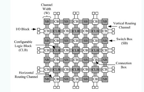
To provide this programmability, FPGAs consist of configurable (or programmable) logic blocks and configurable interconnects between these blocks. this configurable logic and interconnects (routing) of FPGAs make them versatile and flexible, however, they are relatively slow and power hungry compared to similar caliber ASICs with standard cells.
Translated with www.DeepL.com/Translator (free version)

More than 30 years have passed since FPGAs entered the market, and during this long span they have experienced tremendous technological advances and have gained growing popularity.
It is important to note that while similar to PLDs, PLDs (field-programmable gate devices) are limited to hundreds of gates, while FPGAs support thousands of gates.
FPGA Composition
General purpose FPGAs consist of three types of modules, namely
Programmable Logic Units (or CLBs) – responsible for implementing core logic functions.
Programmable Routing – responsible for connecting logic blocks.
IO blocks – connect to the logic blocks via routing and help establish external connections.
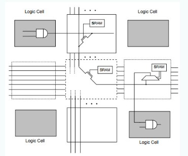
The following is a very broad schematic of a typical internal structure of an FPGA.
Translated with www.DeepL.com/Translator (free version)
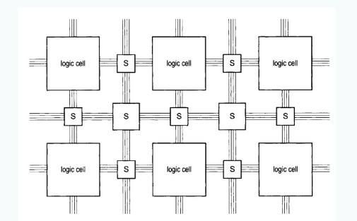
As shown above, the core of an FPGA consists of configurable logic cells and programmable interconnects, and these are surrounded by many programmable IO blocks for communication with the outside world.
1、Programmable Logic Unit
The logic blocks in Xilinx-based FPGAs are called Configurable Logic Blocks or CLBs, while similar structures in Altera-based FPGAs are called Logic Array Blocks or LABs.
CLBs are the basic components of FPGAs that provide logic and storage functions. A basic logic block can be anything from transistors, to a summing gate, to a multiplexer, to a look-up table (LUT), to a PAL-like structure, or even a processor. both Xilinx and Altera use look-up table (LUT)-based logic blocks to implement logic and storage functions.
A logic block can consist of a single basic logic element or a group of interconnected basic logic elements, where the basic logic elements are lookup tables (which in turn consist of SRAM and multiplexers) and flip-flops.
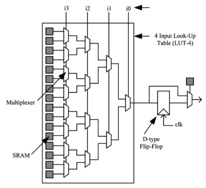
The LUT with “n” inputs consists of 2 nth power configuration bits, which are implemented by SRAM cells. Using these nth power SRAM bits, the LUT can be configured to implement any logic function.
- Programmable Routing
If the computational function is provided by a logical block, the programmable routing network is responsible for interconnecting these logical blocks. The routing network provides interconnections from one logic block to another and between logic blocks and IO blocks to fully implement custom circuits.
Basically, a routing network consists of connecting wires with programmable switches that can be configured using any programming technique. Basically, there are two types of routing architectures, which are
Island routing (also known as mesh routing)
Hierarchical routing
In island routing architecture, logical blocks are arranged in a two-dimensional array and interconnected using a programmable routing network; this type of routing is widely used in commercial FPGAs.
In addition, many logical blocks are restricted to a set of local connections, and the hierarchical routing architecture takes advantage of this feature by dividing logical blocks into groups or clusters. If logical blocks reside in the same cluster, hierarchical routing connects them to a lower hierarchy.
If the logical blocks reside in different clusters, then the routing is done at a higher level of the hierarchy.
Application-based FPGA Types
Field programmable gate arrays are divided into three categories based on the application, such as low-end FPGAs, mid-range FPGAs, and high-end FPGAs.
Low-end FPGAs; these types of FPGAs are designed for low power consumption, low logic density and low complexity per chip. Examples of low-end FPGAs are Altera’s Cyclone family, Xilinx’s Spartan family, Microsemi’s Fusion family, and LatTIce Semiconductor’s Mach XO/ICE40.
Mid-range FPGAs; these types of FPGAs are the best solution between low-end and high-end FPGAs, and they are developed to strike a balance between performance and cost. Examples of mid-range FPGAs are Altera’s Arria, Xlinix’s ArTIx-7/Kintex-7 family, Microsemi’s IGL002, and Lattice Semiconductor’s ECP3 and ECP5 families.
High-end FPGAs; these types of FPGAs are developed for logic density and high performance. Examples of high-end FPGAs are Altera’s StraTIx series, Xilinx’s Virtex series, Achronix’s Speedster 22i series, and Microsemi’s ProASIC3 series.
FPGA Programming Techniques
There are many reprogrammable architectures for FPGAs, but the most common programming techniques responsible for this reconfigurable architecture are
SRAM
EEPROM/Flash memory
AnTI-Fuse (inverse fuse)
Other techniques include EPROM and Fusible Link, but they are used for CPLDs and other PLDs and not for FPGAs, so only programming techniques limited to FPGA-related programming are presented here.
1、SRAM
As you know, there are two types of semiconductor RAM called SRAM and DRAM. SRAM stands for Static RAM and DRAM stands for Dynamic RAM. SRAM is designed using transistors and the term static means that the value loaded on the basic SRAM memory cell will remain unchanged until it is intentionally changed or when the power is removed.
The diagram below shows a typical 6 transistor SRAM cell used to store 1 bit.
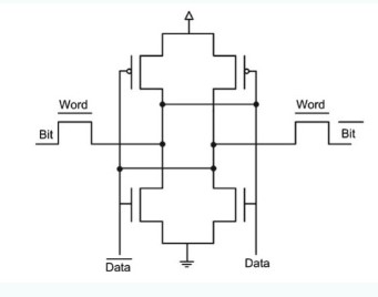
This is in contrast to DRAM, which is a combination of transistors and capacitors. The term “dynamic” refers to the fact that the values loaded into the basic DRAM memory cell remain valid until the capacitor is charged. As the capacitor loses charge over time, the memory cell must be charged periodically to maintain the charge.
Many FPGA vendors implement static memory cells in SRAM-based FPGAs for programming. SRAM-based FPGAs are used to program logic cells and interconnects and have become quite important due to their reprogrammability and use of CMOS technology, which is known for its low dynamic power consumption, high speed, and tighter integration.
- EEPROM/Flash Memory
A similar alternative to SRAM-based programming techniques is EEPROM or Flash-based programming techniques. The main advantage of flash-based programming is its non-volatile nature. Although flash memory supports reprogrammability, the number of reprogrammable programs is very small compared to SRAM technology.
- Anti-fuse
Anti-fuse programming techniques are an old technique for producing one-time programmable devices. They are implemented using a link called an anti-fuse, which has a very high resistance in the unprogrammed state and can be considered an open circuit. When programmed, high voltage and current are supplied to the input. Thus, the anti-fusible wire, which originally connected two metal tracks in the form of amorphous silicon (essentially an insulator with very high resistance), became viable through its transformation into conductive polycrystalline silicon.
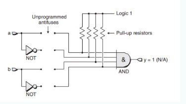
Compared to the other two technologies, the anti-fuse technology takes up the least amount of space, but is only available as a one-time programmable option.
Applications of FPGAs
FPGAs have enjoyed rapid growth over the past decade because they can be used for a wide range of applications. specific applications for FPGAs include digital signal processing, bioinformatics, device controllers, software radio, stochastic logic, medical imaging, computer hardware simulation, integration of multiple SPLDs, speech recognition, cryptography, filtering, and communication coding, to name a few.
And some of the more common FPGA applications include aerospace and defense, medical electronics, ASIC prototyping, audio, automotive, broadcast, consumer electronics, distributed monetary systems, data centers, high performance computing, industrial, scientific instrumentation, security systems, video and image processing, wired communications, and wireless communications.
Summary
In fact, in the early days of the introduction of FPGAs, they were typically used to implement small to medium sized complex state machines and data processing tasks for small data. Over the years, as their complexity and functionality have increased, they have been incorporated into a variety of automotive, consumer and industrial applications.
Initially, FPGAs provided an easy option for prototyping ASIC designs because they could be easily reconfigured to test and try out multiple variants of the hardware before finalizing the main design. However, they functioned as end products with relatively short time-to-market and small implementation costs, so they have been implemented as direct competitors to some ASICs.
As the cost of FPGAs has fallen, they have become a strong competitor for embedded control applications. Today FPGAs can also be used to implement soft-core processors for any microcontroller as well as custom IO functionality.