Circuit boards use different Integrated Circuits (ICs) or chips. Depending on the configurations, these chips can offer different improvements in the board, ranging from the optimization of the components’ functions to the overall transmission of signals.
Dedicated chips called the clock timers or clock circuits are used to carry out the specific functions, relating to transferring signals on the circuit board.
Today, different chip manufacturers have produced an array of these clock timers and you want to know the best ones to buy. In this article, we help you understand how the clock timers or timing Integrated Circuits (ICs) work. You will also learn about the top six (6) clock timers in the market.
What is a Clock Timer?
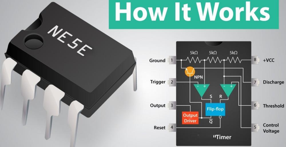
A clock timer or timing Integrated Circuit (IC) is a dedicated chip that helps produce (and manage) signals on the circuit board.
Generally, signals play an important role in the overall functionality of the circuit board, because of the production of varied frequencies and digital square waveforms to match the different target applications.
Choosing the best clock timer or timing IC is a matter of considering the target applications, the cost of the IC and other important factors.
The Best Timing ICs to Buy
Look no farther for the best timing IC to purchase, because we have made a list of some of the best in the market. Here are some of the leading clock timers you want to invest in for your next circuit board project:
1. SI53102-A2-GMR
SI53102-A2-GMR is one of the application specific clock/timing ICs in the market. Manufactured by Skyworks Solutions Inc., it is one of the high-performance 1:2 PCI Express (PCIe) fan output buffers for the Gen 1 to the Gen 4 circuit board specifications.
Generally, clock timers are used in applications that require an excellent timing process, especially when the power is out of the circuit board.
However, when we are looking at the SI53102-A2-GMR solution, it is a different ballgame. According to the manufacturer, this timing IC is exclusive to the embedded applications and consumer electronics.
Features of the SI53102-A2-GMR Timing IC
If you are keen on investing in this clock timer, here are some of the things you want to have in mind:
Specific PCIe Specifications
The support for the PCI Express (PCIe) also includes a specific application or usage. For example, the SI53102-A2- is ideal for the PCIe Gen 2; the SI53102-A3 is ideal for the Gen 3 and Gen 4 PCIe, while the SI53102-A1 is ideal for the PCIe Gen 1.
Power Management
The SI53102-A2-GMR manages power via the two low-power PCIe clock outputs.
Target Applications
Examples of the devices in the embedded and consumer electronics categories supported by the SI53102-A2-GMR are:
- Servers
- Storage devices
- Network Attached Storage
- Wireless Access Points (WAPs)
- Multi-function printers
Excellent Clocking Performance
SI53102-A2-GMR provides you with low-additive-jitter clock buffer. To manage the performance of the timing IC, you are to use the dedicated Skyworks PCIe Clock Jitter Tool.
Technical Specifications of SI53102-A2-GMR
The technical attributes of the SI53102-A2-GMR timing IC include:
- Up to 85-degree Celsius operating temperature.
- Multi-package support, including Digi-Reel, Tape & Reel and Cut Tape.
- Surface Mount Technology (SMT) mounting style.
- Maximum frequency of 100MHz.
- Voltage supply between 2.25 volts and 3.63 volts.
- Input and output ratio of 1:2
2. 9DBL411BGLFT
Renesas Electronics America Inc. manufactures 9DBL411BGLFT. It is a timing IC dedicated to improving the clocking performances of industrial and commercial devices.
Designed as a four-output low-power differential fanout buffer for the Gen 1 to the Gen 3 PCIe, it uses a maximum operating frequency of 150MHz to make these happen. It also supports the QPI PCIe standard.
Key Specifications of the 9DBL411BGLFT Timing IC

Below is a tabular representation of the features that matter the most on this timing IC:
| Attributes | Description |
| Output to output skew | Less than 50ps |
| The jitter for the output cycle-to-cycle | Less than 15ps additive |
| Operating frequency (maximum) | 150MHz |
| Voltage | Between 3 volts and 3.6 volts |
| Input and output ratio | 1:4 |
| Main purposes | PCI Express (PCIe) and Intel QPI |
| Mounting style/type | Surface Mount Technology (SMT) |
| Input method | HCSL |
| Output method | LP-HCSL |
| Operating temperature (maximum) | 70-degree Celsius |
| Supported packages | Available in both the 20-TSSOP and 20-VFQFPN packages. |
Although this timing IC supports a maximum operating temperature of 70-degree Celsius, there is also a variation. The mentioned temperature range is for the commercial applications. If you are working on industrial applications, the operating temperature’s range is between 40-degree Celsius and 80-degree Celsius.
The additional features of the IC include having an individual OE# control output pair, as well as using four low-power differential output pairs.
3. 9DB433AGLFT
Renesas Electronics America Inc. also manufactures the 9DB433AGLFT, only that this time, the timing IC is backward-compatible. It is backward to the PCIe Gen 1 and Gen 2, while supporting the PCIe Gen 3 requirements.
Driven by the powerful differential SRC output pair, it is a zero-delay buffer timing IC optimized for the Express Card applications.
Key Specifications
The major attributes are less than 1.0ps rms phase jitter; less than 50ps output cycle-cycle jitter and less than 50ps output-to-output skew.
The output features comprise:
- Up to 166MHz operation when in the Bypass mode.
- It supports four (4) different 0.7-volt current-mode differential HCSL output pairs.
- Selectable bandwidth
- Between 3.135-volt and 3.465-volt voltage.
- Input and output ratio of 1:4
- Dual mode support, including the fanout mode and the zero-delay buffer mode.
- Up to 110MHz when used in the PLL mode.
The general features include:
- Balancing the power management, especially when the IC is in the Power Down mode. In this case, it supports the undriven differential outputs.
- Multi-device connection via the 3 selectable SMBus addresses. Through these, multiple devices can use the same SMBus segment.
- The jitter is prevented from peaking in the downstream PLLs via the selectable PLL bandwidth.
- Low EMI is tackled by the spread spectrum compatibility, which uses the compatibility to track the spreading input clock.
4. 9DB803DGLFT
9DB803DGLFT is an 8-output differential buffer, designed for the PCI Express (PCIe) Generation 1 and Generation 2 devices. It is typically driven by a differential output pair derived from either of the CK509B, CK410B or CK505 main clock generators.
Below are some of the properties of this timing IC:
- Power Management: It uses a combination of SRC_STOP# and PD# modes derived from the undriven differential outputs.
- The spread includes a +/- 0.25% center spread, between 0 to -0.5% down spread and a general spread spectrum modulation tolerance.
- Dual modes, such as the Bypass and PLL modes. For the Bypass mode, the maximum operation is 400MHz, while that of the PLL mode is between 50 and 100MHz.
- For the output, the IC uses the fanout and zero-delay buffer modes.
- It supports up to 8 0.7-volt current-mode differential output pairs.
- Bandwidth programming is also supported.
The Specifics
The tabular representation below shows some of the specifications of the 9DB803DGLFT timing IC:
| Specifications | Descriptions |
| Phase Jitter | PCIe Gen 2 <3.0/3.1ps rms |
| Outputs cycle-cycle Jitter | <50ps |
| Phase Jitter | PCIe Gen 1 <86ps peak-to-peak |
| Output-to-output skew | <50ps |
Target Application
9DB803DGLFT is ideal for use with the Intel DD800v2, which is a compatible device with the PCIe Gen 1 and the Gen 2 support. The Intel DD800v2 also matches the Differential Buffer Specifications.
5. 9ZXL0831AKLFT
9ZXL0831AKLFT is a low-power 8-output differential buffer and timing IC, optimized to match the specifics of the Intel DB800ZL.
By meeting the above performance requirements, it maintains the low-drift QPI/UPI applications. It also ideal for the PCI Express (PCIe) Gen 1 to Gen 3.
Features of the 9ZXL0831AKLFT Timing IC
The output characteristic is that it has an 8-LP-HCSL output pair. That being said, here are some of the circuit’s additional attributes:
Advanced PLL Mode
The PLL mode’s operation supports both the 100MHz and the 133MHz operating temperatures. That makes it ideal for the QPI and the PCIe applications.
Compact Size
To ensure that the IC functions optimally, the 9ZXL0831AKLFT uses a compact design. In addition to allowing the IC to fit into the circuit board, it also aids in the power management.
Besides, the IC uses low-power push-pull outputs to balance the power supply.
The major space-saving feature of the IC is the compatibility with the 48-pin VFQFPN package.
Technical Properties
The IC’s technical attributes include:
- Up to 70-degree Celsius operating temperature.
- It uses HCSL for the output and Clock for the input.
- Voltage supply between 3.135 volts and 3.465 volts.
- Less than 50ps cycle-to-cycle jitter.
- Less than 50ps input-to-output delay variation.
- It has less than 65ps output-to-output skew.
Applications
The major applications or use cases for the 9ZXL0831AKLFT IC Z-buffer are:
- PCI Express (PCIe)
- Buffer for Romley
- SSD Drivers and;
- Grantley and Purley Servers
6. 841N254BKILF
841N254BKILF is a 4-output clock synthesizer designed for the S-RIO 2.0 and 1.3 reference clock applications. Powered by the FemtoClock NG technology, it leverages that to get a variety of functions, including low-phase noise performance, high clock frequency and high-power supply noise rejection.
Technical Specifications
Here are some of the technical properties for the 841N254BKILF timing IC:
| Specifications | Descriptions |
| Input Formats | Crystal, LVCMOS, LVTTL |
| Operating Temperature | Between 40-degree and 85-degree Celsius |
| Output Formats | LVDS, HCSL |
| Supply Voltage | Between 2.375-volt and 3.465-volt |
| Maximum Operating Frequency | 250MHz |
| Input and Output Ratio | 2:4 |
| Number of Differential Clock Outputs | 4; 2 HCSL outputs and 2 LVDS outputs |
The Relevance of Application Specific Clock and Timing IC Solutions
Clock timers or timing ICs are now integral parts of circuit boards, ranging from Printed Circuit Boards (PCBs) and Microcontrollers (MCUs).
The major contributions they make to the entire circuit board component is that the chips oscillate the board’s signals between the high and low states. The idea is to find a balance for these signals, especially by following the timestamps to coordinate the actions of the circuit board.
1. Reference Clock Failure
Having a timing IC on the circuit board helps to keep the board running and maintaining the accurate clock when the reference clock fails to operate properly. It holds the accurate clock in place, pending when the issue is fixed.
2. Maintaining Synchronization
Clock timers also help to synchronize and manage the same for integrated circuits. The synchronization is maintained across the Global Positioning Systems (GPS), telecommunication devices and handheld devices, especially the handheld variants.
Integral Parts of Clock Timers
Timing ICs do not work solo; they use a couple of components to manage time on the circuit boards. Here are some of the circuit’s integral components:
Clock Generator
It is one of the major time domain managers in a clock timer. It combines with the output buffers, oscillators, output dividers and one or more Phase-Locked Loop (PLLs). The combination aids in the design optimizations for the target applications.
Crystal Oscillator
The crystal oscillator is formed via the combination of the crystal resonator and the oscillation circuit. The combination aids in the formation of the (crystal) oscillator, which aids in the production of a 50% duty cycle square wave.
The square wave becomes the usable oscillating signal and further helps in fixing the clock’s signal at a synchronization mode or to operate at a constant frequency.
Choosing Your Timing IC based on the Type
Clock timers come in different formats, ranging from the crystal to the silicon-based formats. Which of these should you pick for your consumer electronics, industrial and commercial applications?
Here is a breakdown of how each of these works:
Semiconductor-Based Clock Timers
This type of timing ICs use a semiconductor as the base material and tend to include a combination of buffers, and Phase-Locked Loop (PLL) clock drivers.
Silicon-Based Timing ICs
This type of clock timers relies on the clock’s signal distribution to operate the reference clock signal.
Crystal-Based Timing ICs
The full name is Quartz Crystal-based Oscillators. This type of timing ICs is ideal for consumer electronics.
Final Words
Choosing a clock timer should be based on relevant factors like the use cases/applications, operating temperatures and the types. You also want to consider the costs and the number of differential clock outputs the clock timer has before deciding.