There are many articles explaining AUTOSAR storage modules, and this article organizes storage module basics.
Storage Basics
FEE (Flash EEPROM EmulaTIon), i.e. Flash Emulation EEPROM, is a mainstream application nowadays, why should we use Flash Emulation EEPROM?

Here we look at the difference between the two.
Non-volaTIle memory, non-volatile memory, is the memory that can save data after power failure, Flash and EEPROM both belong to this type of memory, but there are still many differences between them, mainly in the following aspects: 1.
- Different erasure methods
Flash: divided into several Pages, when erasing, the whole piece will be erased, when writing, the bit must be 1 to write in, so that every time you modify the data in Flash, you have to erase and then write.
EEPROM: Before writing, it can be modified directly without erasing, it can modify single byte, and the read/write speed is a little slower.
- Number of erasures
Flash is less than EEPROM.
- From the economic point of view
Many chips cancel EEPROM and use Flash to simulate EEPROM instead of EEPROM to reduce cost.
- For different needs
Flash: generally stores some data that is not easy to change, such as some factory data of the vehicle (VIN code), etc. Because these data do not need to be changed from time to time, so it can exist in Flash.
EEPROM: Generally stores some data that can be easily changed, such as DTC in fault diagnosis, if it exists inside Flash it will keep going to erase Flash, and the erase area is larger, which is not good for operation.
FEE: In MCU there is a non-volatile memory we call Data Flash , in AUTOSAR FEE/FLS specification, data is stored in Data Flash by DATA FLASH simulating EEP.
Basic concepts of Flash
Page, Sector, Block

Page:
It is composed of several bytes and is the smallest unit for reading and writing, for example, Page:8 bytes, which means that even if you write one byte to DATA FLASH, it will take up this much space as Page.
Logical SecTIon:
Logical sector, the smallest unit of erasure, consists of several Pages, for example, Logical SecTIon :2K means the smallest unit of erasure is 2K Bytes.
Physical Section:
A physical sector is composed of several logical sectors. For example, if the Physical Section :20K, then it is composed of 10 logical sectors, and a Physical Sector contains several Logical Sectors.
Block.
Generally, a block contains multiple sectors and a SubSector of a sector level, and a Bank, Bulk, etc. of a block level.
Block (bank) > sector (sector) > page (page)
Write operation
EEPROMs are usually written and erased in units of a Byte or Word, i.e., erasure is bounded by Byte or Word, which makes EEPROM erasure more independent and free, and does not affect other data. In addition, the erase life of EEPROM is relatively high, up to one million times.

In EEPROM and Flash, where each memory cell holds one bit of information, the default erase state of the memory cell is read as binary 1. Programming the memory cell changes its value from binary 1 to binary 0, and erasing the memory cell changes its value from 0 to 1.
Programming does not work in reverse: only an erase operation can change the value of a memory cell from 0 to 1.
Flash is usually written in Word or Double-Word, but erases are in Block, which is often measured in KB. These are all related to the semiconductor manufacturing process or design characteristics, which also make Flash very high capacity but short erase life.
Flash Memory has the advantages of light weight, low energy consumption, small size, and high shock resistance, but it also has many limitations, mainly as follows.
Need to erase before writing
Flash Memory has certain limitations when writing data. It can only rewrite bits that are currently 1 to 0, and cannot rewrite bits that are already 0 to 1. Only in the erase operation can the whole block of bits be rewritten to 1.
Limited number of block erasures
Each block of Flash Memory has a limit on the number of erasures (from 100,000 to a million), and after a certain number of erasures, the block will not be able to store data reliably and will become a bad block.
In order to maximize the life of Flash Memory, software needs to do Wear Leveling to balance the use of each data block by means of decentralized writing and dynamic mapping. At the same time, the software also needs to perform Bad Block Management (BBM) to identify bad blocks and keep them out of the data storage.
Read/Write Interference
Due to the physical characteristics of the hardware implementation, Flash Memory may cause bit flipping of other bits in the vicinity during read and write operations, resulting in data anomalies. Such anomalies can be recovered by re-erasing, and algorithms such as ECC are commonly used in Flash Memory applications for error detection and data correction.
Charge Leakage
The charge stored in the Flash Memory memory cell, if left unused for a long period of time, can suffer from charge leakage, resulting in data errors. However, this is a relatively long time, usually about ten years. This abnormality is non-permanent and can be recovered by re-erasing.
AUTOSAR standardized memory modules
The storage of NVM data in AutoSAR mainly includes on-chip storage and external storage: on-chip storage, which uses the internal DFLASH for data storage; external storage, which uses external EEPROM for storage, generally invokes SPI, IIC and other communication methods to externalize the EEPROM chip.

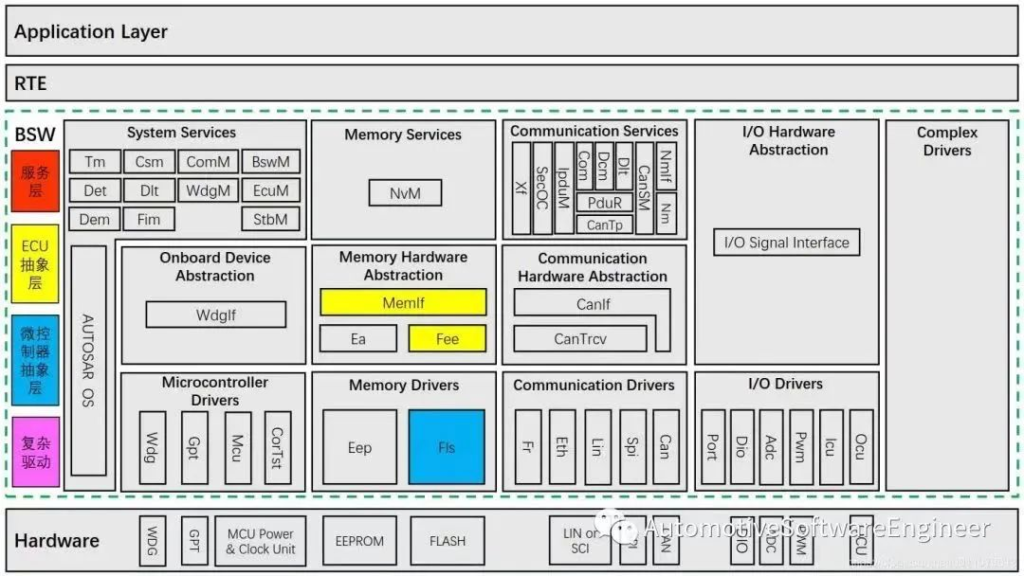
The memory stack in the AUTOSAR layered architecture consists of the following modules, which provide basic memory management services for the upper application layer and the base software.
Non-Volatile Memory Manager – NVM (service layer)
Memory Interface – MemIf (ECU abstraction layer)
Flash EEPROM Emulation – FEE (ECU Abstraction Layer)
EEPROM abstraction – EA (ECU abstraction layer)
Flash Driver – Fls (MCAL layer)
EEPROM driver – Eep (MCAL layer).
NVM mainly provides abstract data storage, reads data in power-up and power-down storage, supports Immediately stored data, and establishes association between ROM and RAM for NV data; MemIf implements the separation operation of stored data blocks in internal Flash or external EEP; FEE implements the abstraction of data blocks in Flash and dynamic data Flash Driver provides the interface to operate Flash; EA defines the memory abstraction and data Layout of external EEPROM; EEP provides the interface and driver to operate external EEPROM.
Detailed summary of each module
NVM Module
Autosar NVM is located in the service layer of the base software and provides various synchronous/asynchronous services for the maintenance (initialization, read, write, control) and management of all NV data.
Both EEPROM and Flash emulation are abstracted to the same type at this layer, and no distinction is made until the MemIf layer, where the upper layer of the NVM module is the RTE, and the lower layer is the interface to the Flash Driver or EEPROM Driver. The application layer will call the functions inside NVM when performing some services related to storage such as writing data or updating DTCs, and NVM integrates interfaces that call Flash emulation and EEPROM respectively according to different needs.
Synchronization mechanism during NvM data operations
The NvM module provides basic synchronous and asynchronous services for the application or base software.
Synchronous services.
Synchronous service is a blocking service call in which the program polls whether the service is completed and returns to execution only when the service is completed. the interface of NVM is called directly in the APP to operate on the data, such approach is not recommended to use the shared RAM Block operation, and the consistency of RAM Block data is ensured in NVM (mainly synchronous CRC mechanism is implemented).

Asynchronous services.
An asynchronous service is a non-blocking service call where a request for a service is placed in a queue and notified to the upper level service for completion via a callback routine configured during block configuration.
The NVM defines a RAM Mirror for data exchange with the APP. When the APP calls NvM_WriteBlock to write data to the RAM Block, the data can still be modified because it has not yet been written to the final Nv Block, and when the NVM data operation NvMWriteRamBlockToNvM is called When the NVM data operation NvMWriteRamBlockToNvM is called, the data is copied to the internal Mirror, and finally the data is written to the Nv Block.

NVRAM data manipulation Block
The operation of data in NvM is generally called Basic storage objects, and Basic storage objects are the smallest unit of storage in NvM.

Memory Service unifies the management of data elements by abstracting them into blocks, and all the functions of NvM are based on the block as a unit.
The blocks managed by NvM include four types of NVRAM blocks, namely NV Block, RAM Block, ROM Block, and Administrative Block.

NV block
is the basic structure for storing NV variables, which is located in non-volatile memory and used to store non-volatile data.
RAM Block
Since writing and reading NV variables is a relatively slow operation, and the application layer logic cycle is too fast. It is obviously not appropriate to directly manipulate the NV block, so before reading or writing, we suggest a Ram space of the same size to manipulate, use, and store the NV values that have not been written or read.
ROM block
Used to store default values to replace NV block data in case of corruption.
Administrative block
The Administrative block is mandatory for NV RAM and contains the attributes, status and error information of NV RAM block related to NvM data management of DataSet type, which can manage the write protection of NV block and the error and status information of last data operation. It is not visible to the application layer.
The management of NvM data consists of three main types of management.
NVM_BLOCK_NATIVE
NVM_BLOCK_REDUNDANT
NVM_BLOCK_DATASET
Native NVRAM block
is the simplest form of Block, this type includes.
1 NV Block, 1 RAM Block, 1 Administrative Blocks

NVM_BLOCK_REDUNDANT
The type of Block contains two NV Blocks, one RAM Block and one Administrative Blocks, and the data stored in the two NV Blocks are backed up to each other, which improves data security.

NVM_BLOCK_DATASET
The Block type can be configured with multiple NV Blocks or ROM Blocks as required and select the operation object by index, which improves the flexibility of the system. The location of each DataSet can be obtained by Administrative Blocks, and NvM can read the selected ROM Block.
The Dataset NVRAM type can be designed to store a data in NvRAM with a certain cyclic offset as needed, and each storage location can be different to achieve an extended lifetime for NvRAM.
MemIf Module
The Memory Abstraction Interface (MemIf) serves as the interface abstraction layer, providing NvM with functions to access Fee/Ea modules, which are abstracted into hardware-independent modules.
MemIf abstracts the relevant interfaces of Fee and EA into MemIf interfaces for NvM access through Device Id.
MemIf can manage both EA and FEE, identified by the DeviceId configuration attribute of the NvM Block, when accessing the corresponding Device Api :
Device ID 0 for EA and Device ID 1 for Fee
FEE module

Fee (Flash Eeprom Emulation), as the name implies, is Flash emulation of Eeprom. So why not use Eeprom directly, or why Flash needs to emulate Eeprom.
Flash and EEP are both non-volatile memory (Non-Valatile Memory) and there are several differences.
Cost
EEP is much more expensive than Flash for the same amount of storage space, so generally Flash space is larger than EEPROM space on MCUs.
Erase method
Flash takes Page as unit, when erasing, it must be erased according to Page as unit, while when writing, it can only write 1, that is, from 0->1, so if you want to rewrite a Byte of a Page, you must first read all the contents of the Page to Ram, then rewrite the corresponding variable in Ram, then erase the Page, and finally write the modified value of Ram to the Page. Page, that is, the following three steps are needed: Read->Change->Write
Eeprom supports direct modification according to Byte
Fee, that is, the Flash write operation, through software simulation into EEP.
Emulation of EEP writing method
Fee operates DataFlash through the Fls module, which has the following physical characteristics.
DataFlash has the following physical characteristics: Write by page, write data must be an integer multiple of the physical page, otherwise bytes must be made up.
The data must be written to an integer multiple of the physical page, otherwise byte completion is required. The minimum erase unit is the whole physical sector.
The write unit of Fee is Block, which is inherited from NvM Block, and the Fee Block Header data is added to the NvM Block data to form Fee Block.
The Fee Block is written to the block according to the principle that the address is first when it is written first, and the next block is written to the block in the next order. This ensures that no erasure is required for each write.
Fee Page Flip Mechanism
Fee divides the Flash space into two logical sectors, one as Active Sector and one as Inactive Sector, which are composed of one or more physical sectors.
At any given time, there can only be one Logical Sector in the Active Sector. Only when the Active Sector, how to write the next Block, or reach the configured remaining space, then a page flip operation will be performed.
The paging operation will generally go through the following steps:
Write the latest data of all Blocks to Inactive Sertor
Erase Active, set Inactive Sector to Active
Note that the page flip operation here does not move all the data from Active Sector to Inactive Sector, but moves the latest data of all Blocks to Inactive Sector.
Assume that our MCU has two sectors in Data Flash, and mark the two sectors as logical sector 1 and logical sector 2 respectively.
Suppose we want to use Flash to emulate EEPROM to store DTC, we all know that DTC is a very small data, but the update may be more frequent, as follows.

First of all, logical sector 1 is blank and waiting for us to write data, it belongs to the working slice (Actived).
Assuming that Flash can write 8 bytes at one time, we can divide it like this: the first 4 bytes to store the DTC logo, the next 4 bytes to store the specific DTC, every time the DTC is updated, we will update the data to the space that has not been written to, until logical sector 1 is full, we will copy the latest DTC data into logical sector 2, and then erase the whole logical sector 1. sector 2), and then erase the whole logical sector 1.
At this time, the status of logical sector 1 (logical sector 1) becomes (Not Actived) pending working sector, logical sector 2 (logical sector 2) becomes (Actived) working sector, wait for logical sector 2 (logical sector 2) to be full and then copy the latest data into logical sector 1 (logical sector 1), and then erase logical sector 2 ( logical sector 2), so back and forth repeatedly, the general workflow is like this.
Fee initializes the read address
Fee provides the address management mechanism, Fee will implement the record of the current address and status of all Blocks in Ram, and will update this address when the Block writes new data.
These addresses are mainly used by Fee to read Block data.
Before the initialization of Fee, these Block addresses are unknown, so it is necessary to get the current Blcok addresses from Flash traversal during the initialization phase of Fee.
EA Module
Since EEP can support direct writing, the block addresses stored in Eep are fixed. The EA module is the EEPROM hardware abstraction layer and operates the EEPROM hardware by accessing the API provided by the lower Eep module.
The EEPROM has the following physical features: it can be written byte by byte without performing data erase operations before writing.
Ea determines the specific hardware storage address for each block and divides the storage space so that NvM can operate the data in the EEPROM hardware by completing the address mapping of the corresponding block through Ea when performing read/write services.
EA Address Management
By obtaining the type and length of the NvM blocks, Ea allocates the address space for each block according to its length, starting from address 0 and working backwards.
EA Block Write Management
The EA Block contains the block status identification bit, which is stored in Eeprom, and the field can determine whether the current Block is valid or not.
If the identification bit is found to be invalid in the read task, the MEMIF_BLOCK_INVALID failure status is returned directly to the upper layer;
If the identification bit is not found to be a valid/invalid value, the MEMIF_BLOCK_INCONSISTENT failure status is returned directly to the upper layer.
FLS Module
The Flash driver provides hardware-independent access to Flash memory and provides service drivers for reading, writing and erasing Flash.

Review Editor: Tang Zixhong