In the aforementioned article, the digitisation process of the analogue compensator for BUCK circuits, we discussed the digitisation of the analogue compensator, in fact, the first important part of the digitisation process is the sampling of the feedback by the ADC, this article will focus on some of the problems caused by the ADC sampling frequency, and then discuss the corresponding solutions.
I. The impact of ADC sampling frequency on the power loop bandwidth

Figure 1 Basic structure of ADC sampling
In the ADC module, a suitable clock is generally selected and divided to generate a suitable clock as the ADC sampling and conversion clock frequency, and there will be a power supply as the reference power supply for ADC conversion, quantization of analog signals, such as AVDD 3.3 V. The ADC module contains a dedicated ADC core and a shared ADC core, the dedicated ADC core is fixed to connect to a certain ADC The dedicated ADC core is fixed to a particular ADC sampling channel and does not require high sampling times, while the shared ADC core is connected to a different ADC sampling channel, which inevitably involves switching between ADC channels. In Figure 1, we can see that the analogue signal will be sampled after entering the ADC sample channel, which will generate a certain delay, and the sampled signal will be converted by the ADC, which will also consume a certain amount of time, and the result will be sent to the ADCBUF register to be processed by the software, or used by the digital filter or digital comparator. The specific performance of the ADC will be discussed in more detail in a later article and will not be explored too much here.

Figure 2 The meaning of sampling in an ADC
Generally speaking, the sampling and conversion of an ADC requires a certain trigger signal. When the trigger occurs, the ADC either starts converting directly or starts sampling and converts after the sampling is finished, which is related to whether the ADC channel is connected to a dedicated core or a shared core. The time between each sample is the ADC’s sampling interval Ts. After conversion by the ADC, the analogue signal is converted to a discrete digital signal, and these numbers are based on the ADC’s reference voltage and the ADC’s bit accuracy to indicate the size of the analogue signal being sampled.
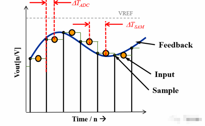
Figure 3 ADC sampling interval and ADC sampling conversion delay
When each time the ADC is triggered, a time is needed to complete the conversion and interrupt request, and then the ADC result is obtained from the ADCBUF in the ADC interrupt. This part of the time delay, there will be some measures in the chip hardware will make this part of the delay as small as possible, in order to leave enough time for the loop control algorithm. It is important to note here that after each sample, the previous sample result is maintained until the next sample, which is the zero-order holdover ZOH.


Figure 4 The concept of ZOH
The Baidu encyclopedia explanation of ZOH, as shown in Figure 4, is the simplest type of sample keeper, where the signal value between each sample interval is constant and its first order derivative is 0. This is where the zero-order keeper comes from, which reduces the digitally sampled signal back to a continuous signal.

Figure 5 Phase loss due to sampling frequency
Understanding the delay caused by ADC sampling, and the zero-order keeper characteristics of ADC sampling, we can look at the phase loss caused by ADC sampling in loop control, as shown in Figure 5, when ADC triggered sampling is performed at 50% of duty cycle, it enters the control loop calculation at the rising edge of the green waveform, and the duty cycle is initially updated at the next cycle, then the phase loss caused at this point is as follows , and

Where fx is the loop control bandwidth and fsample is the sampling interval frequency, so when the sampling frequency is very large relative to the bandwidth, this phase loss will be relatively small, but in reality, the sampling frequency can only be set to the maximum power supply switching frequency (for fixed frequency converters) to ensure that the duty cycle is updated once per switching cycle, so in order to minimise the phase loss caused by the ADC So in order to minimise the phase loss caused by the ADC, we need to set the bandwidth to a suitable value, such as the commonly recommended 1/20 switching frequency, and the phase loss caused by the ADC is 18C.

Figure 6 Optimizing the ADC trigger moment to optimize phase loss
When we change the ADC trigger time to 1/2 of the duty_off time, we let the duty cycle update as soon as we get the calculation result in the next cycle, then we can reduce the phase loss to half of the original, as follows

When the proposed design fx is 1/20th of fsample, the phase delay due to ADC sampling is 9C.
II. Mixing effect of ADC sampling and the solution
Imagine why we recommend that the sampling frequency and bandwidth be kept at a multiple of 1/20? In fact, it is because in sampling science, there is a Nyquist sampling law, where the Nyquist frequency represents the sampling capability corresponding to the sampling frequency.
Sampling must be sampled at a certain rate, and the sampling frequency indicates the rate of sampling. When the sampling frequency is higher, the more accurate the sampled signal is, and when the sampling frequency is twice the frequency of the signal of interest, the frequency of the reduced signal will not be distorted, but there will be distortion in the signal amplitude.
To ensure that the signal frequency is not distorted, we need the signal frequency to be lower than the Nyquist frequency, and to ensure that the signal amplitude is not distorted, we need the signal frequency of interest to be 1/5, or even 1/10th, of the Nyquist frequency. We therefore recommend that the loop bandwidth is set to 1/20th of the sampling frequency (1/10th of the Nyquist frequency) to reduce the effect of the Nyquist frequency on the phase.
Next, we analyse what happens to the signal reduction at different sampling frequencies?

Figure 7 Signal reduction at high sampling frequencies
When we use 9 times the frequency of interest to do the ADC sampling, then we can see from Figure 7 that the sampled signal is reduced to be closer to the original continuous signal.
When we use the Nyquist frequency fn to sample the frequency signal of interest, we find that the sampled signal, in addition to the original signal frequency, is found to be a low frequency signal in the restored signal, and that the signal amplitude itself is significantly distorted after the zero order hold.

Figure 8 Signal distortion due to lower sampling frequency

Figure 9 Signal distortion caused by using 1/2 the signal frequency to sample the signal
When we use half the signal frequency to sample the original signal, we find that the signal undergoes very severe amplitude distortion and a significant low frequency signal is introduced into the restored signal.
The above analysis shows the importance of the sampling frequency to accurately sample and restore the signal. In general, an ADC sampling a signal above the Nyquist frequency will bring in a low frequency false signal which, if picked up by the MCU, will make a wrong command judgement. Therefore, we must avoid it.

Figure 10 Illustration of the mix-and-match effect
As shown in Figure 10, when we assume a sampling frequency of 100Hz, then the Nyquist frequency corresponding to the sampling frequency is 50Hz. Sampling all signals above 50Hz will bring in a low frequency false signal, e.g. 70Hz will bring in 30Hz, 160H will bring in 40Hz, 510Hz will bring in 10Hz, etc. The frequency of the real signal and the low frequency signal mixed in We will not discuss the calculation of the relationship between the real signal and the mixed low frequency signal here, but will consult the relevant information if you are interested.
Since we don’t want overlapping signals to occur, how do we eliminate them? Some people say that a digital filter is recommended, but this is often unrealistic because the MCU cannot distinguish between the low-frequency aliased signal and the real signal, so it filters them all out, and then it is obviously not reasonable to filter out the useful signal. The correct approach, in general, is to filter out all signals above the Nyquist frequency as far as possible before the sampled signal enters the MCU, and with some attenuation, so that no aliasing frequencies are generated, and the common way of filtering is to use RC filters.

Figure 11 Anti-aliasing filter design 1
The ADC will generally have a sample hold capacitor CHOLD, which can be found in the specification, as shown in Figure 12, with a typical value of 18pF for the shared core and 5pF for the dedicated core. This is very important for shared cores, because shared cores will be connected to different input channels, and the voltage of each channel will be different, if not handled properly, it will generate crosstalk between different voltage channels and lead to sampling errors or reduce accuracy.

Figure 12 ADC main structure parameters

Figure 13 Internal structure of the ADC’s analogue input channels
From the ADC’s internal structure, we can see that, in addition to the signal source impedance RS above the analog channel, there are a series of impedances inside the ADC, such as the connection resistor RIC of 300ohm and the sampling switch resistance RSS of 44ohm, so these resistances will lead to a longer charging time for the hold capacitor, and in order to get an accurate sampling voltage, the sampling time needs to be increased appropriately.

Figure 14 Anti-aliasing filter design 2
When the filter capacitance C is determined, we can find the resistor value selection based on the RC turning frequency. As the sampling frequency is the switching frequency, the Nyquist frequency is half of the switching frequency, we hope that the input signal at the Nyquist frequency can have 20db attenuation, then the RC turning frequency should be set to 1/10 of the Nyquist frequency, as in Figure 14, the resistor R can be determined.
To conclude, the design of a digital compensator can be better understood by analysing two typical problems posed by ADC sampling and by discussing their solutions.