If there is a gap in the reference plane, and then the signal crosses that gap, it will produce many undesirable properties in the PCB. For example.
EMI emission increase, EMI immunity impairment, crosstalk increase, deterioration of signal rise time, etc.
But, you say there is an impact on the impact? We still need to see to believe, right?
Next, let’s take a look at the actual test data!
Reference plane with gaps, will generate common-mode currents, which will increase EMI emissions
When there is a gap in the reference plane below the signal, may lead to common mode (CM) interference currents on the system cable, which leads to radiation EMI emissions.
The test system is shown in the figure below.

First, a small oscillator operating at about 30 MHz with a signal edge rate of about 2 nanoseconds and an amplitude of about 3 V peak-to-peak is coupled to the test board pictured above via a short BNC coupler (the guess is that the one inside the green box is the oscillator and the coupler should be on the back, since the side of the BNC socket core is now directly opposite in the picture).
Then, a pair of 2 meter long wires are clamped to the reference plane on either side of the board via alligator clips.
Finally, the CM current generated in these wires is measured by a pair of matched current probes.
A close-up of the test board, generator, and current probes is shown below.

The figure below shows the common mode current measured on a 2 meter long wire, the left side is the result of a solid reference plane, the right side is the result of a reference plane with a gap (I feel that the figure, should not be labeled current1 and current2, instead of current and voltage?) . It can be seen that the CM current measured by the wire with a gap in the reference plane is larger.

Reference plane with gaps will make the PCB EMI immunity degradation
The test system is shown in the figure below.
The test board is still the same test board, but at a distance of 20 cm from it, there is an electrostatic gun, the low-voltage electrostatic discharge (ESD’s).

On the left side of the figure below, the interference signal received by a conductor wired on a solid plane is shown. The amplitude of the signal caused by radiated interference is about 100 mV, which is not enough to disrupt the performance of most digital circuits.
On the right side of the figure below, the interference signal received by a conductor with a gap in the reference plane increases in amplitude to about 3v . is sufficient to cause damage to the function of most digital circuits.

This demonstrates another detrimental effect on the signal conductor produced by routing on the slit in the reference plane, i.e., easier reception of interfering signals.
This is because the return path created by the signal conductor and around the edge of its gap in the reference plane forms a large loop, and this large loop constitutes an efficient antenna that effectively picks up the induced radiated interference.
A reference plane with gaps can be a source of crosstalk
Another problem often caused by alignment through the reference plane is excessive coupling (or crosstalk) between the conductors across the gap.
This is shown in the figure below. Part of the test board above has a wire about 12 cm long (about 50 Ω) running through a 5 cm long gap in the reference plane. A 300 mV signal with a rise time of about 300 ps is then injected into this wire.

The waveforms at the terminals of the 47ohm load resistors (nodes 1 and 2) are shown on the left side of the figure below, while the voltages at the reference plane break at nodes 3 and 4 are shown on the right side of the figure below. The peak voltage in the right figure, with an amplitude of almost 100 mV, indicates that the return flow of the signal through the path around the gap will have a relatively high impedance.

Normally, when the distance between the wires is more than 10h, there is no influence on each other.
But due to the existence of this gap, even if the two wires are 1 cm apart, it can lead to serious crosstalk. The voltage at junction 3,4 in the above figure will be coupled to the other wires.
This is because, in this case, the two conductors must share a common return path (i.e. common impedance) around the edge of the gap in the reference plane.
It causes a change in signal rise time
Even if the gap in the reference plane is relatively small and the rise time is approximately 300 ps, the signal on the conductor crossing the gap in the reference plane may experience significant transition (rise/fall) time distortion (posing a signal integrity problem).
A test signal with a rise time of approximately 300 ps is applied directly from the signal generator through a BNC coupler to two conductors on the test board, with one path routed in a continuous plane and the second path across a 5 cm gap in the plane.

In the figure above, the rising edges of the two signals measured at the terminal are depicted. The signal with a continuous reference plane exhibits a significantly faster edge rate and slight overshoot, while the rate through the plane gap is slower and the overshoot is filtered out.
The reason for the slower edge rate of the signal across the gap is that the return path in its reference plane is forced around the edge of the gap. In addition, the impedance discontinuity in the return path when crossing the gap results in reflection of the higher frequency components of the signal.
This distortion is intolerable from the point of view of signal integrity and functionality.
Segmentation of the reference plane generates radiation
Using 3D simulation software, the following three cases are simulated.
case1: microstrip line, the reference plane is a real plane, PCB size of 400X800X10mil, line width of 5mil.
case2: strip line, two reference planes are solid plane, PCB size of 400X800mil, the thickness of the upper and lower media are 10mil, line width of 5mil.

case3: strip line, one reference plane is solid plane, the other plane has a gap, the PCB size is 400X800mil, the thickness of both the upper and lower dielectric is 10mil, the line width is 5mil, but there is a 50mil wide gap in the lower reference plane.
The dielectric constant of the board, are 4.5.
The specific structure is shown in the figure below, and the right side is the reflow distribution on the reference plane. It is found that as a ribbon line, although there are reference planes on the top and bottom, if there is a gap on one of the reference planes, it will also have an impact on the performance of the ribbon line.
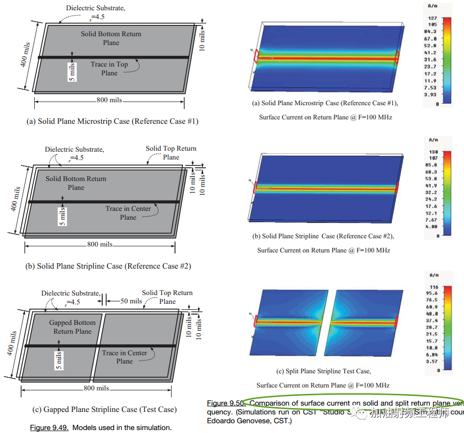
In the figure below, it is shown that the current is discontinuous at the gap and a significant enhancement of the H and E field distributions occurs. This indicates that wave propagation does occur in the gap.
