Application of T6963CFG based LCD in embedded system
In the development and application of embedded systems, the choice of low-cost, high-performance LCD devices has always been the goal of designers. The T6963CFG is an LCD controller produced by TOSHIBA, which can be used for different sizes of LCDs. The HS240128 display from Shenzhen Han Sheng uses this LCD controller, which has a resolution of 240×128 and a self-scanning circuit, with text display, graphic display and mixed graphic display functions.

2 T6963CFG Control Commands and Timing
The T6963CFG is an LCD controller for use with large-scale LCD drivers and data memories. The controller has 8 interface lines for parallel data, read/write control, mode selection, and brightness and backlight control, and can be easily connected directly to a wide range of processor models or microcontrollers. 128 character word mode is built into the T6963CFG; external expansion memory of up to 64 KB (32 KB for the HS240128 display) is used for display buffers, such as text, graphics, and custom character areas. The LCD display window can be easily moved within the display buffer.
2.1 Control commands and status words
The T6963CFG command words have three basic formats.
Format 1: Data1 Data2 Command Code
Format 2: Data1 Command Code
Format 3: Command code
When using format 1, you need to write one byte at a time in the order of data 1, data 2 and command code. If format 3 is selected, only the command code is written. Before reading data or writing data to the LCD, a status check is performed. Only if the LCD is allowed to do so can the corresponding operation be performed. The status words and their functions are shown in Table l.

2.2 Interface signals and timing
The HS240128-1 display is packaged with 21 interface signal lines.
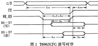
C/D: command/data (high/low) selection signal;
CE: chip select (low) signal;
WR: Write (low) signal;
RD: Read (low) signal;
D0 to D7: Data signal;
FS: Font select signal (high: 6×8, low: 8×8);
FG: Case safety ground;
VSS: GND (ground);
VDD: Power supply for logic circuit and LCD (5 V);
VD: Drive voltage adjustment input (brightness);
VEE: LCD drive power supply (output, -15 V);
RST: reset (low) signal;
K: Backlight (ground);
A: backlight (5 V).
LCD interface control signal read and write timing as shown in Figure 1. The timing of each control signal can be achieved by the microcontroller’s general-purpose input-output (GPIO) interface emulation, for example, when C/D is high, CE is low, WR is high and RD is low, the status word of T6963CFG can be read from the data line (D0 to D7).
3 Hardware interface circuit in embedded system
Usually LCD products have corresponding hardware interface circuits, but the types vary. LCDs with self-scanning circuitry and mixed text, graphics and text display functions can be easily connected to commercially available embedded microcontrollers or microcontrollers, such as the Phlips LPC2104, 2119, etc. The S3C44B0X is a cost-effective embedded system-on-a-chip solution from Samsung that uses the ARM7TDMI core and integrates a rich set of peripheral components on-chip, especially for cost- and power-sensitive applications. Although the S3C44BOX has integrated LCD control logic, the HS240128 display control interface has built-in control circuitry, which can be easily mated with the rich GPIO port resources (71) of the S3C44BOX. In this system design, PD0 to PD7, PE0 to PE2, and PG4 to PG5 are selected as the control and data lines of the LCD. The circuit connection is shown in Figure 2.

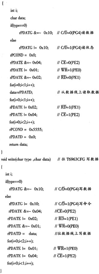
According to the read/write timing of T6963CFG and the corresponding circuit mapping, the function of read/write operation is.
4 Display control and program design
4.1 Display buffer setting
The display buffer can be divided into the system memory display buffer and the LCD display buffer. Of course, the system can also set only the LCD display buffer, and the program can only operate on the LCD display buffer. Usually the LCD display buffer is set in the I/O interface circuit, for example, the display buffer size of HS240128 is 32 KB. Depending on the need, the LCD display buffer can define one, two or three different display zones, for example, text zone, graphics zone and custom character font zone. The size of each zone can be customized as shown in Figure 3. The LCD controller can automatically output and refresh the display information to the screen from the Chinese text and graphic areas of the LCD display buffer, as shown in Figure 3. The display position of the screen and the position of the display buffer have a mapping correspondence.

The display buffer is usually set in the system memory to standardize the program design and improve the efficiency. The program first reads/writes the display buffer in the system memory, and then updates the data to the LCD display buffer. The system memory display buffer is divided into text area and graphics area, and this design sets 8 KB text area and 16 KB graphics area. In the character mode, this area can map 17 display pages, and in the graphics mode, the graphics area can map 4 display pages.
4.2 Character and Graphic Display Processes
4.2.1 Character display process
In the character mode, the HS240128-1 is equipped with 128 commonly used character patterns. By writing the corresponding character codes 00H to 7FH in the specified text display buffer, the LCD can output characters [1]. The LCD display also provides an extended character function with character codes from 80H to FFH, and its character code (8×8 dot font) needs to be written in advance into the font buffer for custom characters. In the application, the font size (1: 6×8 or 0: 8×8) is selected by controlling the FS pin. In the 6×8 mode, the screen can display 40 characters in one line, and in the 8×8 mode, 30 characters in one line. The whole screen can display 16 lines of characters.
In the character mode, the HS240128-1 is equipped with 128 commonly used character patterns. By writing the corresponding character codes 00H to 7FH in the specified text display buffer, the LCD can output characters [1]. The LCD display also provides an extended character function with character codes from 80H to FFH, and its character code (8×8 dot font) needs to be written in advance into the font buffer for custom characters. In the application, the font size (1: 6×8 or 0: 8×8) is selected by controlling the FS pin. In the 6×8 mode, the screen can display 40 characters in one line, and in the 8×8 mode, 30 characters in one line. The whole screen can display 16 lines of characters.
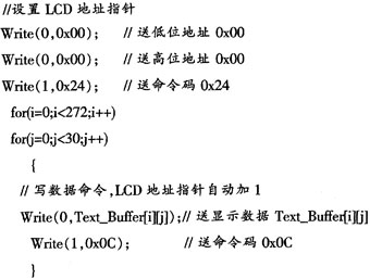
The system memory text buffer has a mapping relationship with the LCD text display buffer. The data format is set according to the screen format size. For example, a line of 30 characters corresponds to 30 consecutive bytes of memory. A screen (page) of 16 lines corresponds to 480 bytes of continuous memory. If the memory text buffer is 8 KB, 17 pages can be mapped (a total of 272 lines), and its buffer is set to: Text_Buffer[272][30] (two-dimensional array of ranks), the process of transferring the data in the memory text buffer to the LCD text buffer can be realized by the following code.
The LCD controller automatically scans and displays the first page of the 17 pages of data sent from memory. If you want to display the second page or other pages, just reset the starting address of the text area to the LCD controller, so the LCD can start displaying from any position in the display buffer. For example. For example, if the display starts from the second line, the LCD text area start address should be 30 (0x001E).
The process of setting the text area start address is as follows.

4.2.2 Graphical display process
The HS240128-1 controller T6963CFG automatically scans and displays the information in the graphics buffer. The system memory graphic display buffer and LCD graphic display buffer has a mapping relationship, and its data format is set according to the size of the screen format.
For example, a line of 240 dots corresponds to 30 consecutive bytes of memory. A screen (page) of 128 lines corresponds to 3,840 bytes of memory contiguity. The memory graphics buffer is set to 16 kB, mapping the LCD screen to 4 pages (512 lines in total). The memory graphics buffer is set to: Graph-ic_buffer[512][30] (array of rows), then the process of transferring the data from the memory graphics buffer to the LCD graphics buffer can be implemented by the following code.

In addition, by setting the starting address of the graphics area to achieve the screen scrolling function, each time a line of scrolling, the graphics area to begin to modify the address increment of +30. For example, the graphics from the second line of display. The address of the graphics area sent to the T6963CFG controller should be 0x201E, i.e. the first address of the graphics area is 2000H+30=0x201E.
The process is as follows.

4.2.3 Chinese character display process
There is no Chinese character library in HS240128-1, so the display of Chinese characters requires a user-defined character pattern to be written to the LCD graphic display buffer, and the display position can be mapped according to the display page. The Chinese character pattern is 16 x 16 dot matrix format (32 bytes). Users who need 16×16 Chinese characters can get them from general Chinese character extraction software, so we will not repeat this article.
4.3 Programming Flow
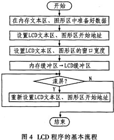
When programming the HS240128, the data is first prepared in the memory display buffer and written to the LCD buffer, and the LCD automatically implements the scan display function. To implement the screen scrolling function, simply modify the start address of the LCD text area and graphics area. The basic flow is shown in Figure 4.
5 Conclusion
This paper systematically introduces the working principle of T6963CFG controller and LCD hardware and software application interface, discusses in detail the application method of dot matrix LCD and design examples in embedded system, and hopes to provide reference for embedded system developers in selecting and using LCDs. The method described in the paper has been well applied in some embedded system designs.
.
4.1 Display buffer setting
2.2 Interface signals and timing