Printed circuit boards (PCBs) are the foundation of electronic devices, providing a platform for a device’s components and interconnections. They help transform complex circuit diagrams into organized, reliable systems. Comprised of layers of conductive material, typically copper, and an insulating material such as fiberglass, these boards have revolutionized the electronics industry since their inception in the early 20th century.
PCBs come in various forms depending on the application and complexity of the circuit. There are single-sided PCBs with just one layer of conductive material, double-sided PCBs with conductive material on both sides, and multi-layer PCBs with several layers insulated by a substrate material. Each type has its specific advantages and applications, ranging from simple electronic devices like calculators to advanced systems like aerospace equipment.
In the manufacturing process, designers use computer-aided design (CAD) software to create a schematic representation of the circuit, which is then translated into a physical PCB with etching, drilling, and component mounting. Innovations in the industry have allowed for increasingly smaller components and higher-density connections, enabling the development of more compact and powerful electronic devices.
Key Components of Printed Circuit Boards
Substrate Material
The base or foundation of a printed circuit board (PCB) is the substrate material, also known as the dielectric layer. A common substrate material is FR-4, which is made from woven fiberglass and epoxy resin. The choice of material heavily influences the board’s overall performance, including its rigidity, thermal conductivity, and electrical properties. Other substrate materials include:
- FR-1: Phenolic paper
- FR-2: Paper-based synthetic resin
- FR-3: Cotton paper laminate
- Aluminum: Commonly used for high heat dissipation applications
Copper Layers
Copper layers form the electrical pathways, or traces, on a PCB. There are three main types of copper layers:
- Single-sided: Copper is coated on one side of the substrate material.
- Double-sided: Copper is coated on both sides of the substrate material and often connected through vias.
- Multilayer: Two or more copper layers are separated by insulating layers and connected through vias.
The thickness of the copper layer is measured in ounces per square foot (oz/ft²) and can vary depending on the current-carrying requirements of the circuit.
Solder Mask
The solder mask is a thin layer of polymer added over the copper layer to protect it from oxidation, corrosion, and accidental short circuits during soldering. It is usually green but can come in various colors, like blue, red, or black. Additionally, the solder mask leaves exposed areas around the pads and vias, allowing for component soldering.
Silkscreen
A silkscreen layer is applied on top of the solder mask and contains human-readable information that aids in component identification, orientation, and debugging. It typically consists of alphanumeric characters, symbols, and outlines representing the components and their locations on the board. The most common silkscreen colors are white, black, and yellow.
PCB Manufacturing Process
Design and Layout
The first step in the PCB manufacturing process is the Design and Layout. Engineers use specialized software to create a digital representation of the circuit board. This design includes the placement of components, traces, vias, and pads required for the final product. Once complete, the design is exported as a set of files that will guide the manufacturing process.
Etching
Etching is the process of removing excess copper from the PCB, leaving only the required traces and pads. This is achieved using chemical solutions that dissolve the unwanted copper, while preserving the remaining material. The PCB is submerged in the etching solution, and the specific areas exposed to the solution are determined by a pre-designed mask. The result is a precise and accurate layout of the electronic circuit.
Drilling Holes
After etching, the next step is Drilling Holes. Holes are essential for mounting components on the PCB, as well as providing pathways for electrical connections between different layers. A specialized drilling machine is used to create the required holes, with accuracy and precision. Drill sizes and locations are determined by the design files previously generated during the design phase.
Assembly and Soldering
Assembly and Soldering is the process of attaching components to the PCB. Components are placed on the board, and held in place with solder paste or adhesive. Soldering is performed either manually or using automated machines such as reflow ovens or wave soldering machines. This process allows for strong, reliable connections between components and the PCB.
Testing and Quality Control
The final stage in the PCB manufacturing process is Testing and Quality Control. Each board must be thoroughly tested to ensure proper functionality and compliance with specific standards. Various techniques are employed, such as visual inspections, automated optical inspections (AOI), and electrical-testing methods such as flying-probe or in-circuit tests (ICT). Any defects discovered during testing are addressed, and the process is repeated until the final product meets the required quality standards.
Types of Printed Circuit Boards
Single-Sided
Single-sided printed circuit boards (PCBs) are the most basic type, consisting of a single layer of conductive material on one side of the substrate. Components are mounted on one side and connected by the conductive traces. These boards are often used in simple electronics due to their low cost and ease of manufacturing. However, they can be limited in complexity and routing options.
Double-Sided
Double-sided PCBs have conductive layers on both sides of the substrate, connected by vias (small holes). This design allows for more complexity, as components and connections can be placed on both sides of the board. Double-sided boards are a common choice for more demanding applications and offer increased routing density, allowing for more compact designs.
Features of double-sided PCBs:
- Two conductive layers
- Vias connect the layers
- Increased routing density
Multi-Layer
Multi-layer PCBs consist of three or more conductive layers, separated by insulating materials and connected by vias. These boards can be more complicated, but they provide greater design flexibility, increased component density, and improved electrical performance. Multi-layer PCBs are commonly used in high-end electronics, such as smartphones and computers, where space is at a premium.
Advantages of multi-layer PCBs:
- Increased design flexibility
- Greater component density
- Improved electrical performance
PCB Design Software
Printed circuit boards (PCBs) require careful design and planning before they can be manufactured. To accomplish this, engineers use specialized software to aid in creating and verifying their designs. Several popular PCB design software packages are available to choose from, each with its advantages.
EAGLE is a widely used PCB design software that offers a range of functionality, from schematic capture to PCB layout. Developed by Autodesk, it has a robust library and an easy-to-learn user interface. It also has good community support and is available in different versions to suit your needs.
KiCad is a popular open-source PCB design software that caters to both beginners and experienced users. With its advanced features, it is suitable for creating high-quality layouts for professional designs. It supports various file formats, allowing designers to import and export files from different software.
Another choice is Altium Designer, known for its powerful features and comprehensive design solutions. It is widely used in the industry and is particularly known for its high-speed design capabilities, 3D visualization, and extensive component libraries.
Some key aspects to consider when selecting a PCB design software are:
- Ease of use: Choose a software that meets your skill level and allows for efficient design.
- Functionality: Consider which features are essential for your projects and compare them among the options.
- Pricing: Compare the costs associated with each software to find the best fit for your budget.
- Support and resources: Look for strong community support, tutorials, and access to component libraries.
In conclusion, the choice of PCB design software is crucial in ensuring successful PCB designs. There are several options, such as EAGLE, KiCad, and Altium Designer, which cater to different user needs and preferences.

Advancements and Future Trends
In recent years, Printed Circuit Board (PCB) technology has seen significant advancements, leading to improvements in performance, miniaturization, and cost reduction. Some key trends shaping the future of PCBs include:
-
High-density interconnect (HDI) PCBs: HDI technology allows for more components to be mounted on a single PCB, increasing functionality without increasing size. This is achieved through the use of microvias, buried vias, and blind vias, allowing for more connections in a smaller area.
-
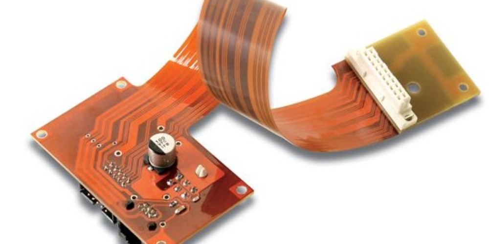
Flexible and stretchable PCBs: With the development of flexible materials, PCBs are no longer limited to rigid structures. Flexible PCBs are bendable, lightweight, and can be used in applications where conventional PCBs would not fit. Industries like wearables, medical devices, and automotive are greatly benefiting from these advancements.
-
Embedded components: By embedding passive components such as resistors, capacitors, and inductors within the layers of a PCB, designers can save space and improve overall performance. This also allows for a reduction in assembly time and enhances signal integrity.
-
Environmentally friendly materials: As environmental concerns rise, PCB manufacturers are focusing on using materials that are less harmful to the environment. For example, replacing traditional FR4 substrates with more eco-friendly alternatives and implementing lead-free soldering techniques.
Looking ahead, the PCB industry is expected to continue innovating to meet the demands of emerging technologies such as the Internet of Things (IoT), electric vehicles (EV), and 5G communication. Some potential developments include:
-
Increased use of AI and automation: AI-driven software can optimize the design and manufacturing processes, resulting in higher efficiency and reduced errors. Automation in PCB assembly can also reduce labor costs and further improve accuracy and reliability.
-
3D printing: As 3D printing technology advances, it may revolutionize PCB prototyping and manufacturing. This can lead to faster turnaround times, reduced costs, and the ability to create highly complex and customized designs.
-
Graphene integration: Graphene, an ultra-thin and highly conductive material, has the potential to greatly improve the electrical properties of PCBs. Its lightweight, flexible, and heat-dissipating qualities make it a promising candidate for future PCB advancements.
In conclusion, the PCB industry is constantly evolving, with new advancements pushing the boundaries of what is possible in electronics design and manufacturing. As emerging technologies continue to shape the future, we can expect to witness even more innovative solutions that further improve the capabilities of printed circuit boards.