Printed circuit board assembly (PCBA) is the process of mounting electronic components onto printed circuit boards (PCBs) to create functional electronic devices. PCBs have become crucial in the world of electronics, ranging from consumer products such as smartphones, computers, and televisions to medical devices, vehicles, and industrial equipment. As the demand for high-performing, compact products continues to grow, so does the need for efficient and innovative circuit board assembly techniques.
The assembly process begins with the design of a PCB, wherein electronic engineers create circuits and layouts that suit the desired functionality. Once the design is finalized, fabrication of the bare PCBs takes place, followed by the assembly of required components such as resistors, capacitors, and integrated circuits. Several methods are employed for this, including surface mount technology (SMT), through-hole technology (THT), or a mix of both, depending on the type of components and their intended application.
Advanced machinery and automation have greatly impacted the PCB assembly industry by improving the speed, accuracy, and consistency of the processes. Automation has also helped minimize human errors, thereby enhancing the quality and durability of the final products. As we continue to rely heavily on electronic devices in various aspects of our lives, the importance of efficient and reliable printed circuit board assembly cannot be overstated.
Printed Circuit Board Assembly Basics
When it comes to printed circuit board (PCB) assembly, understanding the basics is crucial. This section will provide you an overview of key aspects involved in the process, along with essential components and materials, along with the various types of PCBs.
Components and Materials
PCB assembly involves the following components and materials:
- Bare PCB: The foundation for the assembly, made of substrates and copper traces.
- Electronic components: Including integrated circuits (ICs), resistors, capacitors, and connectors.
- Solder: A metal alloy used to create electrical connections between the components and the PCB.
The quality of components and materials is crucial for the performance and durability of the final product.
Types of Printed Circuit Boards
There are several types of PCBs, each designed to suit specific requirements:
- Single-sided PCBs: They have only one layer of copper traces and are suitable for basic electronics and low-cost applications.
- Double-sided PCBs: These have two layers of copper traces, allowing for more complex circuits and a higher density of components.
- Multi-layer PCBs: Designed for advanced applications, these boards have more than two layers of copper traces, providing improved signal integrity and noise reduction.
By understanding the basics and taking these factors into consideration, you can make informed decisions when choosing a printed circuit board assembly provider to ensure the best possible outcome for your project.
Assembly Process
Design and Layout
The printed circuit board (PCB) assembly process begins with the design and layout of the board. This involves selecting the right materials, determining the appropriate size and shape, and arranging the components in an optimized manner. A well-designed layout not only ensures proper component placement but also helps reduce potential signal interference and the probability of manufacturing errors.
Fabrication
Once the design and layout are finalized, the fabrication process commences. This involves creating the actual PCB by bonding layers of copper, insulating material, and other substrates. Photolithography, a process where a photosensitive mask is applied over the copper, is used to etch the desired traces and patterns onto the board. Following the etching process, holes are drilled and plated through, allowing for interconnections between various layers.
Component Placement
The next stage in the assembly process is component placement, where the electronic components are accurately positioned on the PCB according to the design layout. This can be done manually, but for high-volume production, automated placement machines are often utilized to increase speed and accuracy. Surface mount technology (SMT) and through-hole technology are the two common methods used for attaching components to PCBs. The choice depends on the design, component types, and manufacturing requirements.
Soldering
Finally, the soldering process is performed to electrically connect the components to the PCB using solder paste or solder wire. Soldering techniques can vary depending on the type of components and PCB technology used. For surface mount components, reflow soldering is commonly used, where the solder is heated in an oven until it melts and wets the contact points. In the case of through-hole components, wave soldering or selective soldering can be utilized. After the soldering process, inspection and testing are conducted to ensure proper functionality and quality.
Testing and Quality Control
Visual Inspection
Visual inspection is a crucial step in the printed circuit board assembly (PCBA) process. This inspection detects any visible defects on the board, such as:
- Solder bridging: Occurs when solder flows between pads, causing potential short circuits.
- Missing components: Ensures all required components are placed on the board.
- Tombstoning: When components are lifted from the surface during soldering.
To ensure high quality, manufacturers employ both manual inspections by trained personnel and automated optical inspection (AOI) machines. AOI machines use high-resolution cameras, along with image-processing software, to identify defects and ensure proper alignment of components.
Functional Testing
Functional testing is another important aspect of testing and quality control. This step ensures that the assembled PCBs are operating as intended. It runs the board through a series of tests that simulate standard use and measure the response of the components to ensure they meet predefined specifications. Some functional tests include:
- In-circuit test (ICT): Uses a bed-of-nails tester to check for open or short circuits, component values, and functionality.
- Flying probe test: A contact-based testing method that does not require a dedicated test fixture, making it ideal for small production runs.
- JTAG/boundary scan: A non-contact method that relies on embedded test circuits to test interconnects between components.
Functional testing is essential in detecting manufacturing defects and ensuring a high level of product quality for end-users.
Design Challenges and Solutions
Thermal Management
One challenge in printed circuit board assembly is managing heat. Overheating leads to performance reduction and potential failure. To overcome this, the following solutions are used:
- Material selection: Using materials with higher thermal conductivity for better heat distribution.
- Component placement: Spacing out components, particularly heat sources, to avoid concentrated heat areas.
- Thermal vias: Incorporating thermal vias into the PCB design to improve heat transfer to the other side.
By implementing these strategies during the design phase, you can maintain effective thermal management throughout the PCB’s lifetime.

Signal Integrity
Another challenge in PCB assembly is preserving signal integrity across the board. Signal distortion and noise can affect overall performance. To address this issue, designers focus on these factors:
- Impedance control: Matching impedance between the source, transmission line, and load to prevent signal reflections.
- Signal return path: A proper return path should be established, minimizing the loop area to avoid noise and crosstalk.
- Decoupling capacitors: Placing capacitors near the power supply pins helps to maintain signal integrity by filtering out noise.
By incorporating these solutions into your PCB design, you can ensure signal integrity and maintain the high performance of your electronic devices.
Industry Applications
Consumer Electronics
Printed circuit board assembly (PCBA) is a crucial process in the production of consumer electronics like smartphones, computers, and televisions. These electronic devices rely on PCBs to connect and communicate with various components. The demand for smaller, lighter, and more powerful devices has led to advancements in PCB assembly technology, resulting in higher-density interconnects and the use of surface mount technology.
Some key factors that affect the assembly process in consumer electronics are:
- Component miniaturization
- Reliability and performance requirements
- Mass production scale
Aerospace and Defense
In aerospace and defense applications, the stakes are much higher as the failure of PCBs can lead to catastrophic consequences. The requirements for PCB assembly in this sector are:
- High reliability and quality standards
- Durability in harsh environments
- Compliance with strict industry certifications (MIL-STD, IPC Class 3)
The aerospace and defense industries use advanced materials and processes in their PCB assembly to handle the demanding requirements of these applications. Some of these include:
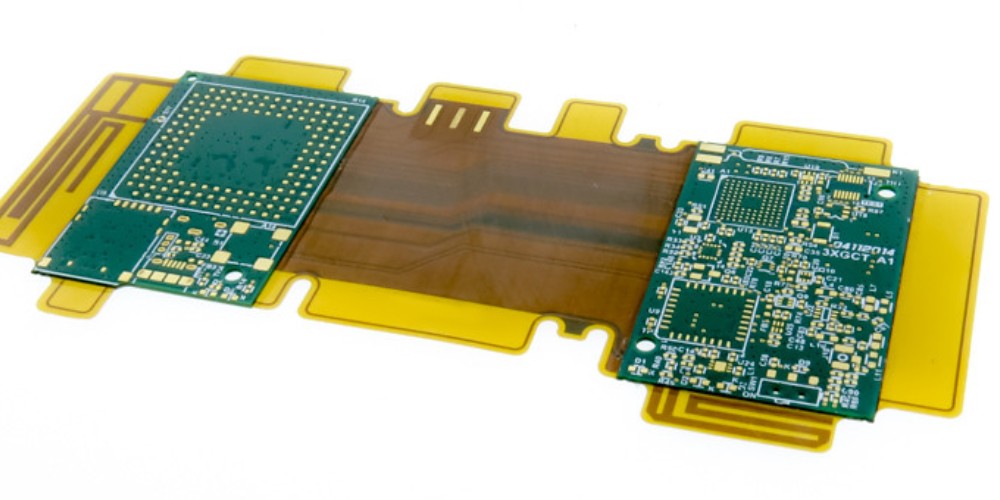
- Rigid-flex PCBs
- High-temperature laminates
- Conformal coatings
By understanding the unique requirements of each industry, PCB assembly providers can offer tailored solutions to ensure the highest level of performance and reliability for the end product.
Future Trends
Rapid Prototyping
Rapid prototyping is a significant trend in the printed circuit board assembly (PCBA) industry. It involves creating prototypes quickly and efficiently, reducing the time to market for new products. Technological advancements, such as 3D printing and computer-aided design (CAD) software, have significantly reduced the time taken to turn an idea into a working prototype.
Some key benefits of rapid prototyping include:
- Faster feedback for design changes
- Reduced development costs
- Shorter time to market
- Improved product quality
Companies that can adopt rapid prototyping effectively will gain a competitive edge in the fast-paced world of electronics.
Flexible Electronics
Flexible electronics is another trend that’s influencing the PCBA industry. This technology enables the creation of bendable and foldable electronic devices, opening up new possibilities in product design. Key advancements in material science and manufacturing processes have made flexible electronic components more durable and reliable.
Flexible electronics offer several advantages, such as:
- Lightweight and thin components
- Conformability to curved surfaces
- Potential for wearable and portable applications
As flexible electronics gain traction, there will be a growing demand for PCBAs that can accommodate these devices. Adapting to this trend will be crucial for PCB manufacturers to remain competitive in the future.