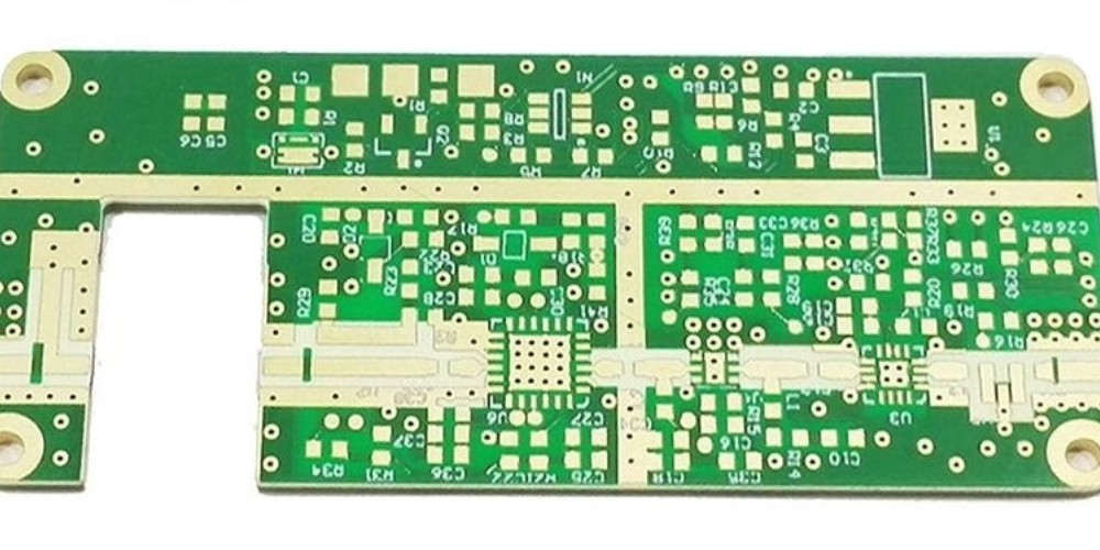
Printed Circuit Board (PCB) fabrication is a critical process in the electronics industry. It involves the creation of PCBs, which serve as the foundation for the assembly of electronic components in virtually all electronic devices. These boards are responsible for providing the electrical connections between the various components and ensuring the device functions properly.
The fabrication process encompasses several steps, including design, material selection, and the actual fabrication process. Designing a PCB begins with creating a schematic of the electronic circuit, followed by translating this schematic into a physical layout that efficiently utilizes the available space on the board. Material selection is crucial, as the chosen materials must be durable, conductive, and compatible with the components being used.
During the fabrication process, the PCB is manufactured in a series of stages, each contributing to the overall functionality and reliability of the final product. These stages include the application of copper layers, etching of the circuit pattern, and the addition of solder mask and silkscreen layers. Each step must be carefully executed to ensure proper electrical connections and minimize the risk of defects or failures in the final product.
Overview of PCB Fabrication
Printed Circuit Boards (PCBs) are essential components of almost every electronic device, ranging from basic consumer products to advanced aerospace and defense systems. This section provides a brief overview of the materials and processes involved in PCB fabrication.
Materials
The primary constituents of a PCB are:
- Substrate: Often made from fiberglass reinforced epoxy resin known as FR-4, the substrate provides a rigid, stable, and non-conductive base for the thin layers of metal and other elements.
- Copper: The copper layer is either affixed to the substrate or created through an electrochemical process. It serves as the conductive path for signal transmission.
- Solder mask: A protective layer of polymer, usually green in color, that is applied on top of the copper layer to insulate and protect the delicate copper traces from environmental hazards and short circuits.
- Silkscreen: An ink layer applied to the surface of the PCB containing component designations, symbols, and other supplementary information to aid in assembly, testing, troubleshooting, and repairs.
Manufacturing Process
The PCB fabrication process consists of several steps and could be briefly summarized as follows:
- Design and layout: Engineers design the electronic circuit and generate PCB layout files using specialized computer software.
- Fabrication: The layout files are sent to a fabrication facility, where the raw materials are processed into the final PCB. Key steps include:
- Substrate preparation: Substrates are cleaned, cut to the desired size, and prepped for copper deposition.
- Copper deposition: A thin layer of copper is either directly applied to the substrate surface or created through an electrochemical process.
- Pattern transfer: The desired pattern of conductive traces, pads, and other features is transferred to the copper layer using UV-sensitive photoresist and UV exposure.
- Etching: Excess copper is removed using chemical etchants, leaving behind the desired pattern.
- Drilling: Holes for through-hole connections and other features are drilled according to the layout files.
- Solder mask application: The solder mask layer is applied over the copper traces, followed by curing.
- Silkscreen printing: Component markings, reference designators, and other useful information are printed onto the solder mask layer.
- Inspection and testing: The fabricated PCB is thoroughly inspected and tested for defects and functionality before moving on to the assembly process.
Designing a PCB
Designing a Printed Circuit Board (PCB) involves many steps to create a functional and reliable end product. Two crucial stages in this process are Schematic Capture and PCB Layout. These steps ensure that the electronic components are interconnected and correctly placed on the board.
Schematic Capture
Schematic Capture is the process of designing the circuit using a software tool. In this stage:
- Designers create a visual representation of their circuit.
- Components such as resistors, capacitors, and ICs are added to the schematic diagram.
- Electrical connections between components are defined using wires and symbols.
- Design rules and constraints are established.
Once the schematic capture phase is complete, it serves as the blueprint for the remainder of PCB design, ensuring that the layout phase meets all necessary requirements.
PCB Layout
The PCB Layout process is where the physical aspects of the board are designed:
- Component placement is determined, taking into account factors like thermal considerations, signal integrity, and mechanical constraints.
- Routing of electrical connections is performed, with attention given to reducing noise, crosstalk, and interference.
- Layers are assigned to specific routing purposes; for example, power and ground planes.
- Design rules are checked and validated to ensure compliance with fabrication and assembly requirements.
After these steps, the PCB design can be sent for fabrication and assembly. Both the Schematic Capture and PCB Layout phases are crucial for a successful PCB design, with attention to details and requirements during each step, resulting in a final product that performs as expected.
PCB Fabrication Techniques
Printed Circuit Board Milling
Printed Circuit Board (PCB) milling is a subtractive manufacturing method. It involves removing unwanted copper from a PCB substrate to create the desired layout. The CNC milling machine or router drives the cutting tool across the substrate, which creates space for necessary traces and components.
Advantages of PCB milling:
- Low-cost: No need for extensive chemical treatment
- Quick: Suitable for prototyping purposes
- Environmentally friendly: Uses less hazardous chemicals
However, PCB milling has some drawbacks:
- Precision: Potential inaccuracies in complex designs
- Limited Capability: Not suitable for producing multi-layer PCBs
Chemical Etching
Chemical etching is a widely used fabrication approach, particularly for mass-produced PCBs. This technique involves applying a chemical etchant — usually ferric chloride or ammonium persulphate — that dissolves unwanted copper from the PCB substrate.
A high-level overview of the process:
- Photoresist Application: A photosensitive layer applied to the copper surface
- Exposure: Expose the PCB to UV light through a mask containing the desired pattern
- Development: Remove the exposed photoresist, revealing the copper to be etched
- Etching: Apply the chemical etchant, removing the excess copper
- Stripping: Remove the remaining photoresist, leaving the PCB pattern in place
Advantages of chemical etching:
- Accuracy: Capable of producing intricate patterns
- Scalable: Ideal for large-scale, high-volume production
Disadvantages of chemical etching:
- Chemical waste: Requires processing and disposal of hazardous materials
- Process time: Longer process compared to milling
Both PCB milling and chemical etching offer unique benefits and drawbacks. Your decision on which fabrication technique to use will largely depend on their distinctive capabilities, intended application and the desired scale of production for your PCBs.

Testing and Quality Control
Functionality Tests
Functionality tests are essential to ensuring that the manufactured PCBs meet the design specifications and function as intended. Some common types of functionality tests include:
-
In-Circuit Testing (ICT): This test method involves using a bed-of-nails fixture to make connections with the PCB’s test points. The fixture is customized to the specific PCB and confirms that components are correctly placed and function as intended.
-
Flying Probe Testing: As a fixtureless test method, flying probe testing involves using moving test probes to make contact with the test points on the PCB. This test method has several advantages, such as flexibility and quicker time-to-test. However, flying probe testing may not be suitable for high-volume production due to longer testing times compared to ICT.
-
Automated Optical Inspection (AOI): AOI systems use cameras to visually inspect the PCB for component placement, orientation, and quality. AOI can detect various defects, such as missing, misplaced, or incorrectly oriented components.
Visual Inspections
While automated tests like AOI are useful for catching manufacturing defects, visual inspections still play a crucial role in quality control. These inspections can be performed using:
-
Manual Inspection: Skilled technicians use magnifying tools to examine the PCB for defects like solder bridges, component misalignments, and other quality-related issues on the boards.
-
X-ray Inspection: By using X-rays, it is possible to inspect the internal structure of the PCB, particularly for hidden solder joints under Ball Grid Array (BGA) components. X-ray inspection helps identify soldering issues, such as voids or short circuits, that may not be visible to the naked eye.
Both functionality tests and visual inspections are critical aspects of PCB fabrication quality control, ensuring that each board functions as intended and meets the rigorous standards of the electronics industry.