OLED driver based on N32G45
1.OLED Introduction
OLED, that is, organic light emitting diode (Organic Light Emitting Diode). OLED is considered to be the next generation of flat panel display emerging application technology due to its excellent features such as self-emitting, no backlight, high contrast ratio, thin thickness, wide viewing angle, fast response time, flexibility panel, wide temperature range, and simple construction and process.
OLED display technology differs from traditional LCD displays by eliminating the need for a backlight and using a very thin coating of organic materials and a glass substrate (or flexible organic substrate) that emits light when an electric current/’ target=’_blank’ class=’arckwlink_none’>current is passed through. And OLED display screens can be made lighter and thinner, with larger viewing angles and significant power consumption savings.
OLED is also known as the third generation of display technology. oled is not only thinner, lower energy consumption, high brightness, good luminosity, can display pure black, and can also be bent, such as today’s curved screen TV and cell phones. Today’s major international manufacturers are scrambling to strengthen the research and development of OLED technology, making OLED technology in today’s TVs, computers (monitors), cell phones, tablets and other fields of application more and more widespread.

The selected OLED screen is 0.96 inch, the driver IC is SSD1306, the driver protocol is SPI. the resolution is 128*64; monochrome screen. The page addressing method is used.
Pin Description
Pin Description
GND Power ground
VCC Power positive (3 to 5.5V)
D0 pin of D0 OLED, clock pin in SPI and IIC communication
D1 pin of OLED, data pin in SPI and IIC communication
RES# pin of RES OLED, used for reset (low reset)
D/C#E pin of DC OLED, data and command control pin
CS# pin of CS OLED, also known as chip select pin
To connect to external devices, the SPI interface has four pins for connection to peripheral devices, as follows.
SCLK: Serial clock pin, the signal is output from the SCLK pin of the master device and input from the SCLK pin of the slave device
MISO: Master input/slave output pin, data is input from the MISO pin of the master device and output from the MISO pin of the slave device
MOSI: Master output/slave input pin, data is output from the MOSI pin of the master device and input from the MOSI pin of the slave device
NSS: chip select pin, there are two NSS pin types, external pin and internal pin. If the internal pin detects a high level, the SPI operates in master mode, and conversely, the SPI operates in slave mode. The user can use a standard I/O pin of the master device to control the NSS pins of the slave device
SPI is a ring bus structure. The master device outputs a synchronous clock signal through the SCK pin, the master device’s MOSI pin is connected to the slave device’s MOSI pin, and the master device’s MISO pin is connected to the slave device’s MISO pin so that data can be transferred between devices. Continuous data transfer between the master and slave devices sends data to the slave device via the MOSI pin and the slave device sends data to the master device via the MISO pin.

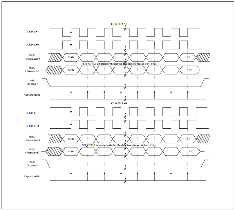
SPI Timing Mode
By setting the SPI_CTRL1.CLKPOL bit and the SPI_CTRL1.CLKPHA bit, the user can select the clock edge along which data is captured.
When CLKPOL = 0, CLKPHA = 0, the SCLK pin will remain low when idle and the data will be sampled on the first clock edge, i.e., the rising edge.
When CLKPOL = 0, CLKPHA = 1, the SCLK pin will remain low when idle and the data will be sampled on the second clock edge, i.e. the falling edge.
When CLKPOL = 1, CLKPHA = 0, the SCLK pin will be held high when idle and the data will be sampled on the first clock edge, the falling edge.
When CLKPOL = 1, CLKPHA = 1, the SCLK pin will remain high when idle and the data will be sampled on the second clock edge, i.e. the rising edge.
Regardless of which timing mode is selected, the timing mode configuration must be the same for both the master and slave devices.
SPI Timing Diagram
2.3 Hardware SPI-related registers and configuration
Taking full duplex as an example, the configuration flow of SPI is as follows.
setting the SPI_CTRL1.SPIEN bit to 1 to enable the SPI module.
write the first data to be sent to SPI_DAT (this write operation clears the SPI_STS.TE flag bit).
Wait for SPI_STS.TE flag position 1, then write the second data to be sent to SPI_DAT register, wait for SPI_STS.RNE flag position 1, read SPI_DAT register to get the first received data, read SPI_DAT register, SPI_STS.RNE flag bit will be cleared to 0. Repeat the above operation to send the subsequent data, while receiving the nth-1st data.
Waiting for SPI_STS.RNE to set to 1 and then reading the last data.
Wait for SPI_STS.TE flag bit position 1 and wait for SPI_STS.BUSY flag bit to be cleared before turning off the SPI module
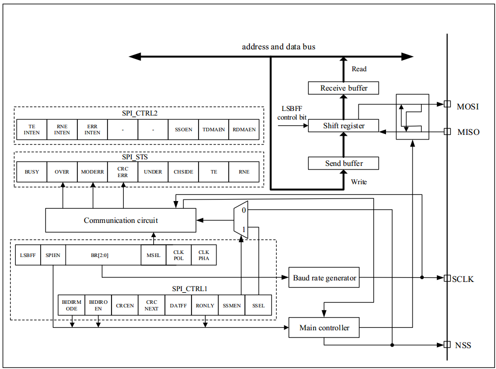
SPI_CTRL1 register
CTRL1 is used to configure SPI operating mode, operating frequency, clock polarity, enable SPI and other parameters.

SPI_STS register
The STS status register is used to determine the data sending and receiving completion status, interrupt flag, busy flag, etc.

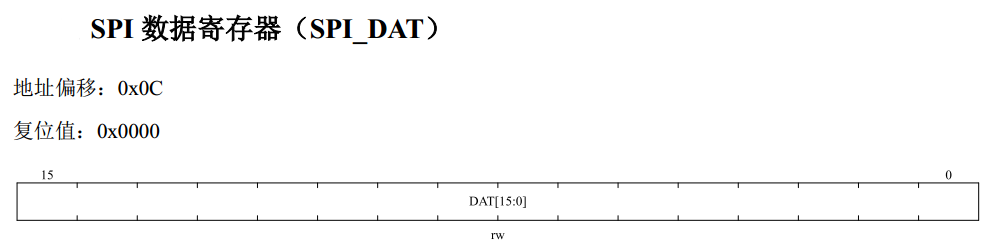
SPI_DAT register
The DAT data register holds the transmitted and received data.
2.4 Hardware SPI Pin Definitions
This development board has 3 hardware SPI (SPI1, SPI2, SPI3) and one QSPI. QSPI supports the standard SPI mode and QSPI is an interface for single/dual/quad SPI peripheral communication. It can work in 2 modes, indirect and memory mapped.
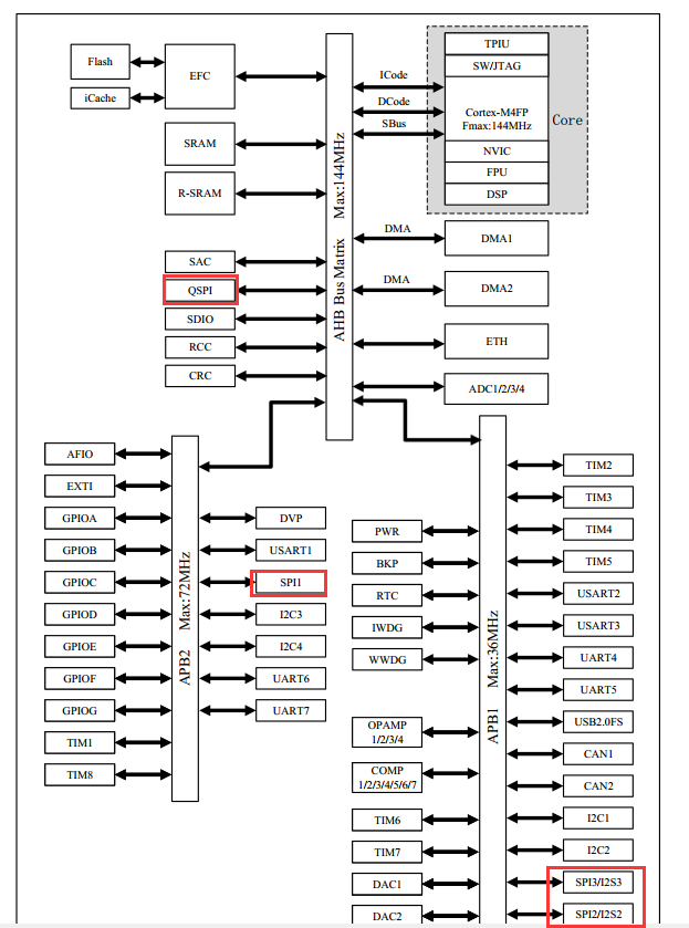
Take SPI1 as an example, drive the OLED screen through SPI1. SPI1 is mounted on APB2, and according to the introduction of SPI_CTRL1 register, the maximum communication speed of SPI1 is 72MHZ/2=36MHZ.
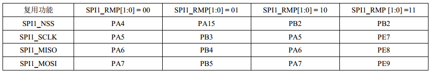
According to the hardware schematic of the development board, PA5 and PA6 have been connected to the keypad, and PB4 and PB5 have been connected to the LED device, so to ensure no interference, SPI1 can be turned on for complete re-imaging, using PB2, PE7, PE8 and PE9 as the hardware interface of SPI1.
SPI1 Redirect Register
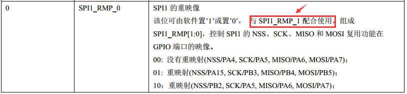
SPI1 hardware redirection is configured through a combination of the SPI1_RMP_0 and SPI1_RMP_1 bits. SPI1_RMP_0 is in bit 0 of SPI1_CTRL1; SPI1_RMP_1 is in bit 18 of SPI1_CTRL3.
The configuration code is as follows.
/*OLED pin initialization ***
**D0 — PE7 clock line, SCLK
**D1 — PE9 data line, MOSI
**RES — PB12 reset pin, low reset, high cancel reset
**DC —PB1 Data command select line
*CS —PB2 chip select line, low selected, high unselected /
**Note: Use hardware SPI1 — maximum speed is 36MHZ, use SPI1’s full re-imaging
*Author: IT_Ashui **/
static void OLED_GPIO_Init(void)
{
//on clock
RCC->APB2PCLKEN|=1<<3;//PB RCC->APB2PCLKEN|=1<<6;//PE RCC->APB2PCLKEN|=1<<0;//AFIO AFIO->RMP_CFG|=1<<0;//SPI1 pin fully redirected AFIO->RMP_CFG3|=1<<18;//SPI1 fully re-imaged //Configure GPIO port GPIOE->PL_CFG&=0x0fffffff;
GPIOE->PL_CFG|=0xB0000000;
GPIOE->PH_CFG&=0xffffff0f;
GPIOE->PH_CFG|=0x000000B0;
GPIOB->PH_CFG&=0xfff0ffff;
GPIOB->PH_CFG|=0x00030000;
GPIOB->PL_CFG&=0xfffff00f;
GPIOB->PL_CFG|=0x00000330;
//SPI1 mode configuration
RCC->APB2PCLKEN|=1<<12;//SPI1 RCC->APB2PRST|=1<<12;//SPI1 RCC->APB2PRST&=~(1<<12);//SPI1 SPI1->CTRL1|=1<<9;//software slave device management SPI1->CTRL1|=1<<2;//master mode SPI1->CTRL2|=1<<2;//SPI1 is buggy, need to enable this bit to use SPI1->CTRL1|=1<<6;//Enable SPI
OLED_CS=1;//chip select pull low
OLED_RES=1;
}
Note: According to the N32 hardware errata guide, there are bugs in the SPI1 hardware when operating in master mode, and the problems are as follows.
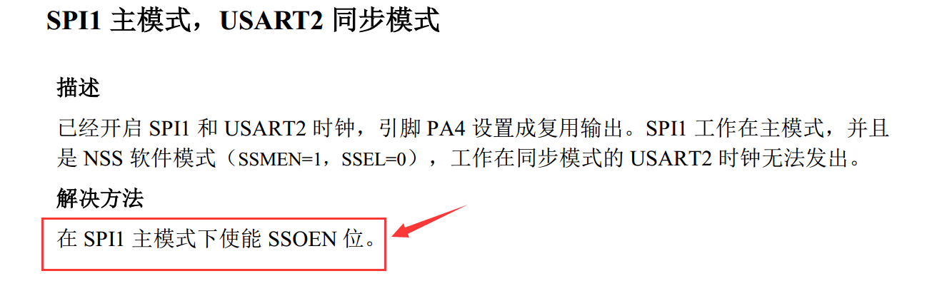
Although this example is a full re-imaging function via SPI1, with the clock line re-imaged from PA4 to PB2, it was tested that not setting SSOEN would cause the send data to fail.
Bottom send a byte function
Since the OLED screen uses a 3-display SPI interface with no host input pin, it is only necessary to implement sending data
/SPI sends a byte ***/
static inline void SPI_ReadWriteByte(u8 data_tx)
{
SPI1->DAT=data_tx;
while(! (SPI1->STS&1<<1)){}//Wait for data sending to complete
}
2.5 OLED-related interface functions
Dot function implementation
To implement the OLED picture, string, Chinese characters and other functions, the core function is the draw point function. However, since this OLED screen is initialized by page addressing, we need to create a cache to facilitate the implementation of the draw point function.
/ drawing point function ***
**
** Formal parameters:u8 x — horizontal coordinates 0~127
** u8 y –vertical coordinates 0~63
** u8 c –0 means no display, 1 means display
**OLED_DrawPoint(50,20,u8 c)
**/
static u8 oled_gram[8][128];// screen buffer
void OLED_DrawPoint(u8 x,u8 y,u8 c)
{
u8 page=y/8;//y coordinate value in the first page
u8 line=y%8;//in the current page on the first few lines
if(c)oled_gram[page][x]|=1<;>
Chinese character display implementation
The OLED itself does not come with a font, so in order to achieve the Chinese character display, you need to take the mold, you can use PctoL2002 to complete the Chinese character take the mold. Of course, you can also make a Chinese character library, burn it into flash and then call the library directly to display it.
/* Chinese character display *
** shape parameter:u8 x,u8 y — the position to be displayed x:0~127,y:0~63
** u8 size — font size
** u8 number — the first few words
/ void OLED_DisplayFont(u8 x,u8 y,u8 size,u8 number) { u16 i=0,j=0; u8 data; u8 x0=x; for(i=0;isize>
Character strings are completed by PctoL2002 for common character modelling, both 16 dot matrix and 24 dot matrix.
/* String display function
u8 x,u8 y — the position to be displayed x:0~127,y:0~63
u8 w,u8 h — character width and height
char *str — the string to be displayed
Return value: return the number of characters displayed
**/
u8 OLED_DisplayStr(u8 x,u8 y,u8 w,u8 h,char *str)
{
u8 x0=x;
u8 cnt=0;
while(str!=”) { if(x0>=127)return cnt; if(y>=63)return cnt; OLED_DisplayCha(x0,y,w,h,(u8 )str++);
x0+=w;
cnt++;
if(x0>=127)//change page
{
x0=0;
y+=h;
}
}
return cnt;
}
Screen clear function
This function mainly realizes screen clearing, which can be achieved from top to bottom, left to right and back to three modes of screen clearing.
/*更新显示*/ void OLED_Refresh2(u8 format) { int i=0; int j=0; u8 flag=0; u8 x=127,y=63; int line=0,row=0; u8 cnt=0; switch(format) { case 1://从上往下 for(i=63;i>=0;i–) { for(j=0;j<128;j++) { OLED_DrawPoint(j,i,0); } OLED_Refresh(); Delay_Ms(100); } break; case 2://从左往右 for(i=0;i<128;i++) { for(j=0;j<64;j++) { OLED_DrawPoint(i,j,0); } OLED_Refresh(); Delay_Ms(20); } for(i=127;i>=0;i–) { for(j=0;j<64;j++) { OLED_DrawPoint(i,j,1); } OLED_Refresh(); Delay_Ms(20); } break; case 3://回字形 i=0; j=0; flag=0; x=127,y=63; line=-1,row=-1; cnt=0; while(1) { if(flag==1)j++; else if(flag==2)i–; else if(flag==3)j–; else i++; if(i>=x && flag==0) { x–; row++; flag=1; } if(j>=y && flag==1) { flag=2; line++; y–; } if(i<=row && flag==2) { flag=3; } if(j<=line && flag==3) { cnt++; flag=0; } OLED_DrawPoint(i,j,0); if(cnt>=1) { cnt=0; OLED_Refresh(); Delay_Ms(50); } if(row>x || line>(y+4)) { break; } } i=0; j=0; flag=0; x=127,y=63; line=0,row=0; cnt=0; while(1) { if(flag==1)j++; else if(flag==2)i–; else if(flag==3)j–; else i++; if(i>=x && flag==0) { x–; row++; flag=1; } if(j>=y && flag==1) { flag=2; line++; y–; } if(i<=row && flag==2) { flag=3; } if(j<=line && flag==3) { cnt++; flag=0; } OLED_DrawPoint(i,j,1); if(cnt>=1) { cnt=0; OLED_Refresh(); Delay_Ms(50); } if(row>x || line>(y+4)) { break; } } break; default: OLED_ClearGram(0x0);//清空缓冲区 OLED_Refresh(); break; } }
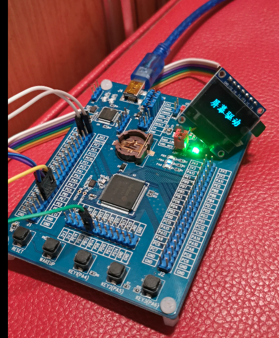
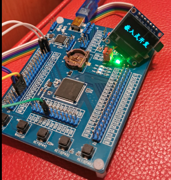
2.6 Overall effect