Many precision analog-to-digital converters (ADCs) today have a serial peripheral interface (SPI) or some serial interface to communicate with controllers such as microcontroller units (MCUs), DSPs, or FPGAs. SPI is becoming increasingly popular because of its simple printed circuit board (PCB) routing and faster clock rate compared to parallel interfaces. Also, ADCs can be easily connected to controllers using standard SPI.

Some new ADCs have SPI, but others have non-standard 3- or 4-wire SPI as nodes because they want to achieve faster throughput rates. For example, the AD7616, AD7606 and AD7606B series have two or four SDO lines for faster throughput rates in serial mode. The AD7768, AD7779, and AD7134 series have multiple SDO lines that are used as SPI power supplies. Users often have difficulty designing microcontroller SPI for ADC configuration and code reading.
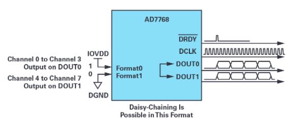
Figure 1. The AD7768 acts as a serial main power supply with two data output pins (14001-193).
Standard MCU SPI Connection to ADC
SPI is a synchronous, full duplex, master/node based interface. Data from the master node or nodes is synchronized on the rising or falling edge of the clock. The master node and the node can transmit data simultaneously. Figure 2 shows a typical 4-wire MCU SPI interface connection.
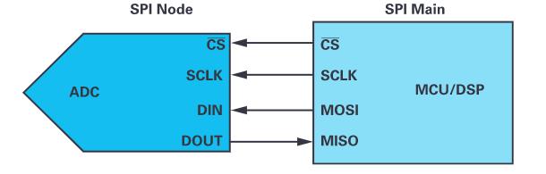
Figure 2. Standard MCU SPI connection to the ADC node.
To start SPI communication, the controller must send a clock signal and select the ADC by enabling the CS signal (usually a low active signal.) Since SPI is a full duplex interface, the controller and ADC can output data simultaneously through the MOSI/DIN and MISO/DOUT lines, respectively. The controller SPI interface gives the user the flexibility to select the rising or falling edge of the clock to sample and/or convert data. For reliable communication between the master nodes, the user must follow the digital interface timing specifications of the microcontroller and ADC chip.
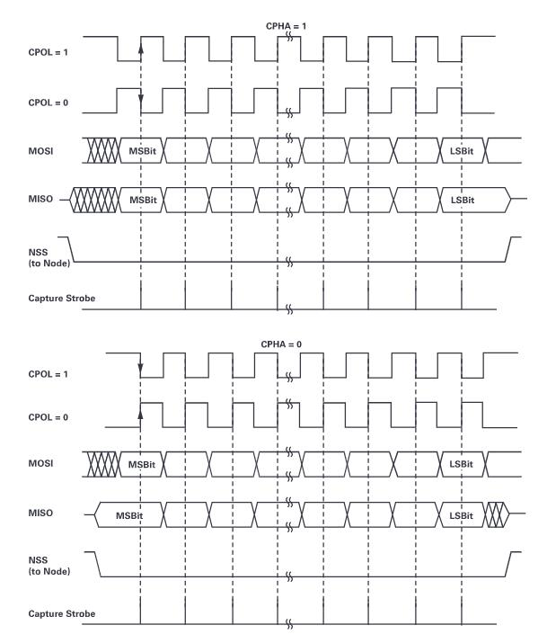
Figure 3. Example of SPI data clock timing diagram.
If the microcontroller SPI and ADC serial interface has a standard SPI timing mode, it is not a problem for the user to design the PCB routing and develop the driver firmware. However, there are some new ADCs with serial interface ports which are not in typical SPI timing mode. it seems impossible for MCU or DSP to read data through the AD7768 serial port (non-standard timing SPI port), as shown in Figure 4.
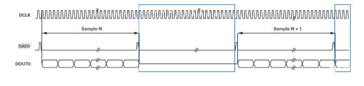
Figure 4. AD7768 format x = 1 x timing diagram output, using DOUT0 only.
This paper will describe the method of operating a standard microcontroller SPI to interface with an ADC that has a non-standard SPI port.
Four different solutions for reading ADC code via the serial interface will be presented.
Solution 1: MCU as SPI node interfacing to ADC as SPI master via one DOUT line.
Solution 2: MCU as SPI node, interfacing to ADC as SPI main line through two DOUT lines.
Solution 3: MCU as SPI node, interfacing with ADC as SPI master via DMA.
Solution 4: MCU as SPI master node and SPI node for reading data on two DOUT lines.
AD7768 using STM32F429 microcontroller SPI to read code through one DOUT line
As shown in Figure 4, when FORMATx = 11 or 10, channels 0 through 7 output data on DOUT0 only. In standard mode, the AD7768/AD7768-4 operates as a master device and streams data to the MCU, DSP or FPGA. the AD7768/AD7768-4 provides data, data clock (DCLK) and falling edge framing signal (DRDY) to the node devices.
The STM32Fxxx family of microcontrollers is widely used in many different applications. the MCU has multiple SPI ports and can be configured as an SPI master or node with typical SPI timing modes. The methods described in the following sessions can also be applied to other microcontrollers with 8-bit, 16-bit or 32-bit frames.
The AD7768/AD7768-4 have 8-channel and 4-channel synchronous sampling sigma-delta ADCs with sigma-delta modulators and digital filters per channel for synchronous sampling of AC and DC signals, respectively. They achieve a dynamic range of 8 dB at a maximum input bandwidth of 108.110 kHz with typical performance of ±2 ppm INL, ±50 μV detuning error, and ±30 ppm gain error. AD7768/AD7768-4 users can weigh input bandwidth, output data rate, and power consumption and select one of three power modes to optimize noise targets and power consumption The flexibility of the AD7768/AD7768-4 makes it a reusable platform for low-power DC and high-performance AC measurement modules. Unfortunately, the serial interface of the AD7768 is not a typical SPI timing mode, and the AD7768 is used as the serial interface master interface. Typically, the user must use an FPGA/CPLD as its controller.
For example, using the 32F429IDISCOVERY and the AD7768 evaluation board. The solution SPI leads are connected as shown in Figure 5. In this setup, all 7768 AD0 channel data outputs are powered by DOUT<> only.
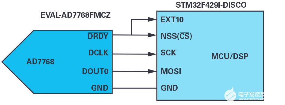
Figure 5. The AD7768 outputs data on DOUT0 to the STM32F429 MCU SPI connection.
Issues to be addressed.
The AD7768 is used as an SPI master device, so the STM32F429I SPI must be configured as an SPI node.
The DRDY high pulse is only one cycle of the DCLK duration and is not a typical CS.
DCLK is output continuously and DRDY is low when all channel data bits have been output.
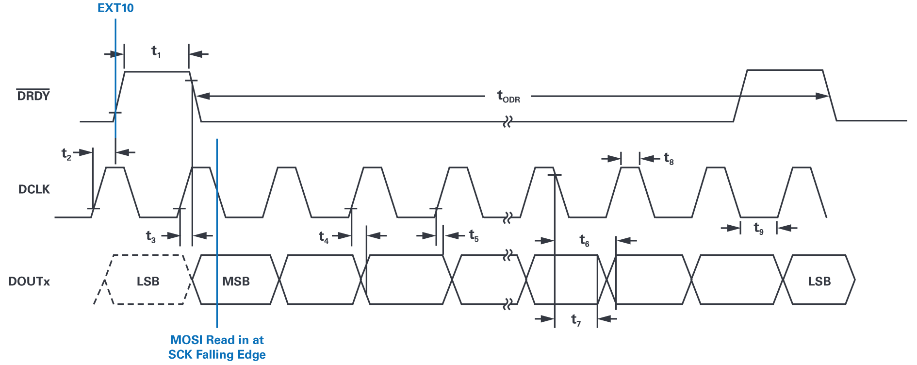
Figure 6. AD7768 data bits are read in the timing solution.
Solution 1: MCU SPI as a node interfaced to the SPI master ADC via a DOUT line
Configure one of the STM32F429 is SPI ports (e.g. SPI4) as a node to receive data bits on the MOSI of the DCLK.
Connect the AD7768 DRDY to the STM32F429 external interrupt input pin EXTI0 and the NSS (SPI CS) pin. the rising edge of DRDY will trigger the EXTI0 handler routine to enable the SPI node to start receiving data bits from the first DCLK falling edge after DRDY goes low. Timing design is critical here.
After receiving all data from channel 0 to channel 7, the SPI should be disabled to prevent reading additional invalid data as DRDY brings the SPI node CS low and DCLK constantly switches.
MCU Firmware Development Notes
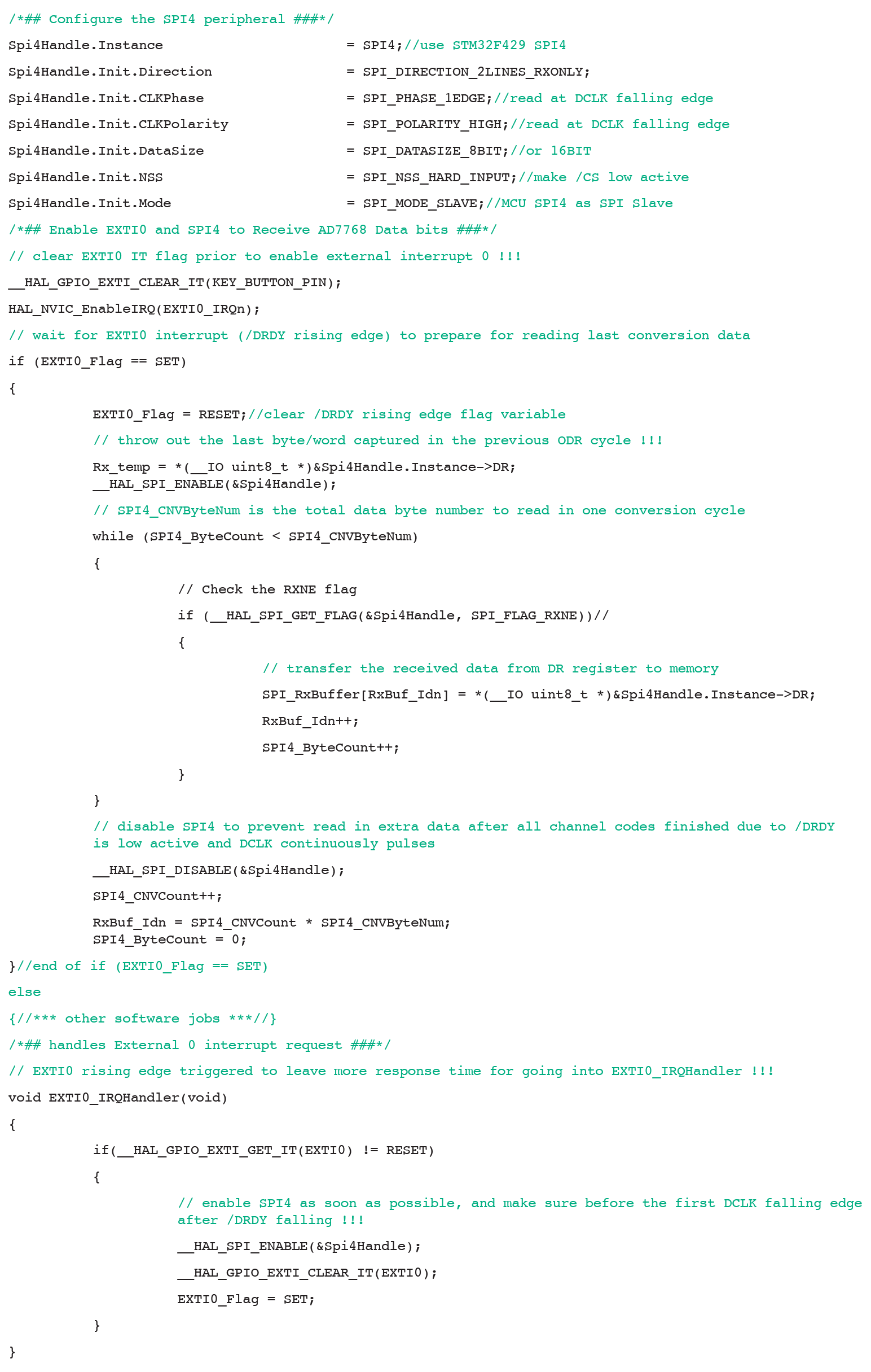
Figure 7. Configuring the SPI4 peripheral.
When software is in interrupt mode, DCLK can run up to 4 MHz and achieve an ODR of 8 kSPS. software should enter the interrupt handler to start the SPI in one and a half DCLK cycles (375 ns). to make it easier for software to enter the interrupt routine, the MCU can read data on the rising edge of DCLK, which can provide an additional half DCLK cycle time. However, since the minimum value of 5DCLK rising to DOUTx invalid is -3 ns (-8 ns with IOVDD = 4.1 V), propagation delay (>|t5|+ MCU hold time) on DOUTx should be added via PCB wiring or buffers.
Solution 2: MCU SPI as a node interfacing to the SPI master ADC via two DOUT lines
In the first solution, only DOUT0 is used to output all 8 channels of data. Therefore, data reads limit the ADC throughput rate to 8 kSPS. As shown in Figure 1, channel 3 to channel 0 outputs on DOUT0 and channel 7 to channel 1 outputs on DOUT4 shorten the data transfer time. The serial line connections are shown in Figure 7. With this improvement, the ODR can easily reach 4 kSPS at DCLK 16 MHz.
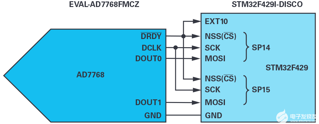
Figure 8. The AD7768 outputs data on DOUT0 and DOUT1 to the STM32F429 MCU SPI connection.
The firmware can use polling mode instead of interrupt mode to reduce the time delay of the DRDY rising edge trigger so that the SPI can receive data. This allows for an ODR of 8 kSPS at DCLK 32 MHz.
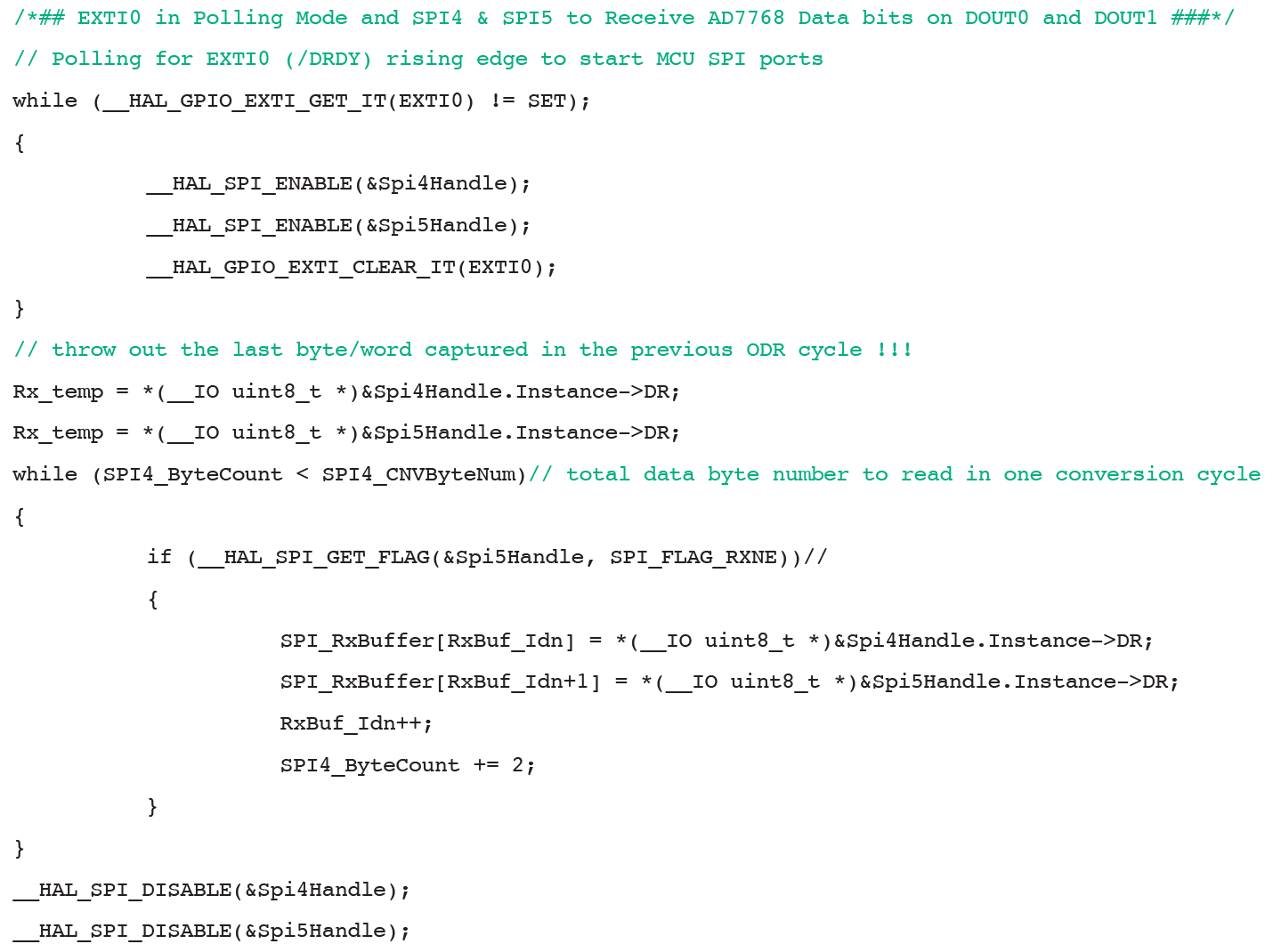
Figure 9. EXTI0 in polling mode and SPI7768 and SPI0 on DOUT4 and DOUT5 receiving AD1 data bits.
Solution 3: MCU SPI as a node interface to the SPI master ADC interface via DMA
Direct Memory Access (DMA) is used to provide high-speed data transfers between peripherals and memory and between memory and memory.DMA allows for fast data movement without any MCU operation. This allows MCU resources to be used for other operations. The following is a design description of the MCU SPI as a node receiving data via DMA.
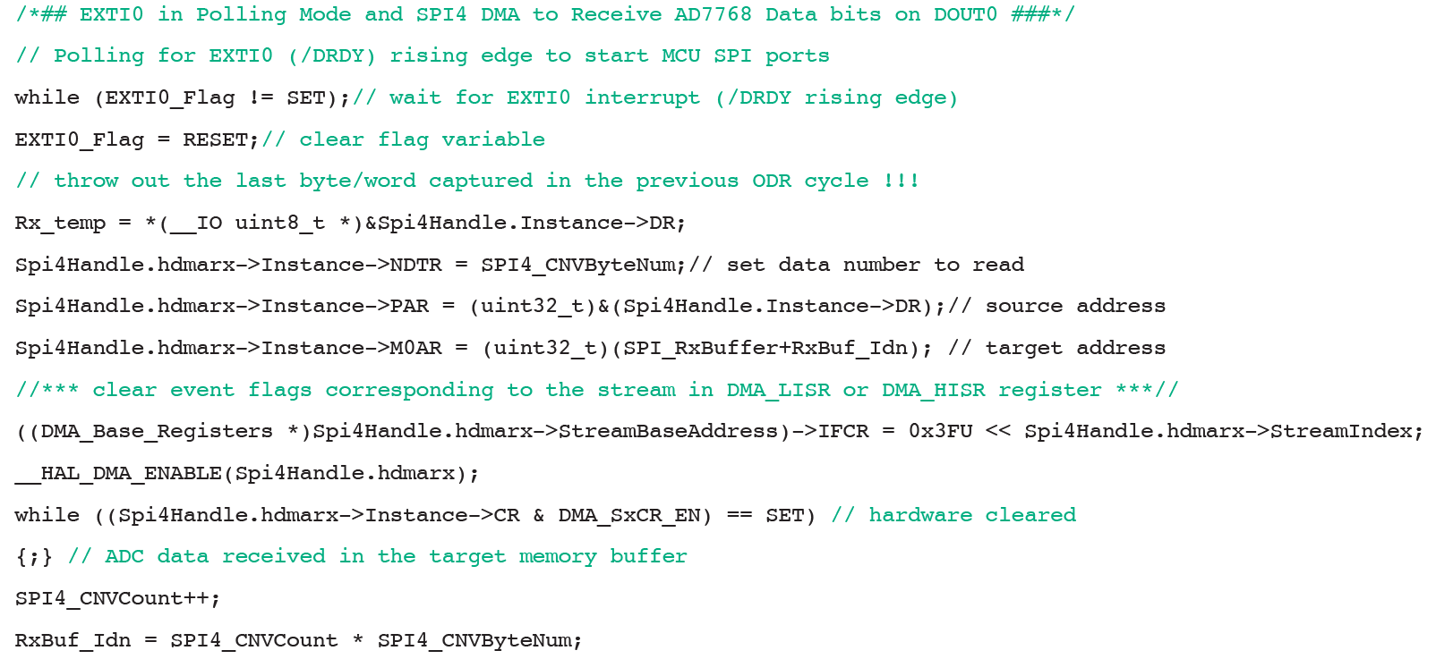
Figure 10. SPI7768 DMA receiving AD0 data bits on EXTI0 and DOUT4 in polling mode.
Solution 4: MCU SPI as master and node to read data on two DOUT lines
High throughput or multi-channel precision ADCs provide two, four or even eight SDO lines for SPI ports, which can reduce code read time in serial mode. For microcontrollers with two or more SPI ports, they can run the SPI ports simultaneously to speed up code reads.
In the following use case, the 32F429IDISCOVERY uses SPI4 as the SPI master node and SPI5 as the SPI node to receive the EVAL-AD7606B-FMCZ data on DOUTA and DOUTB, as shown in Figure 8.
The AD7606B is a 16-bit synchronous sampling analog-to-digital data acquisition system (DAS) with 16 channels, each containing analog input clamping protection, a programmable gain amplifier (PGA), a low-pass filter, and a 7606-bit successive approximation register (SAR) ADC. the AD2B also has a built-in flexible digital filter, a low-drift, 5.7606 V precision reference voltage The AD5B is powered by a single 10 V supply and supports ±2 V, ±5 V, and ±800.<> V true bipolar input ranges when all channels are sampled at 5 kSPS throughput rates.
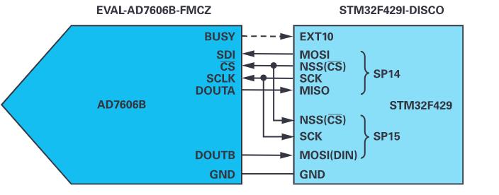
Figure 11. MCU SPI used in master mode and node mode for receiving data on DOUTA and DOUTB.
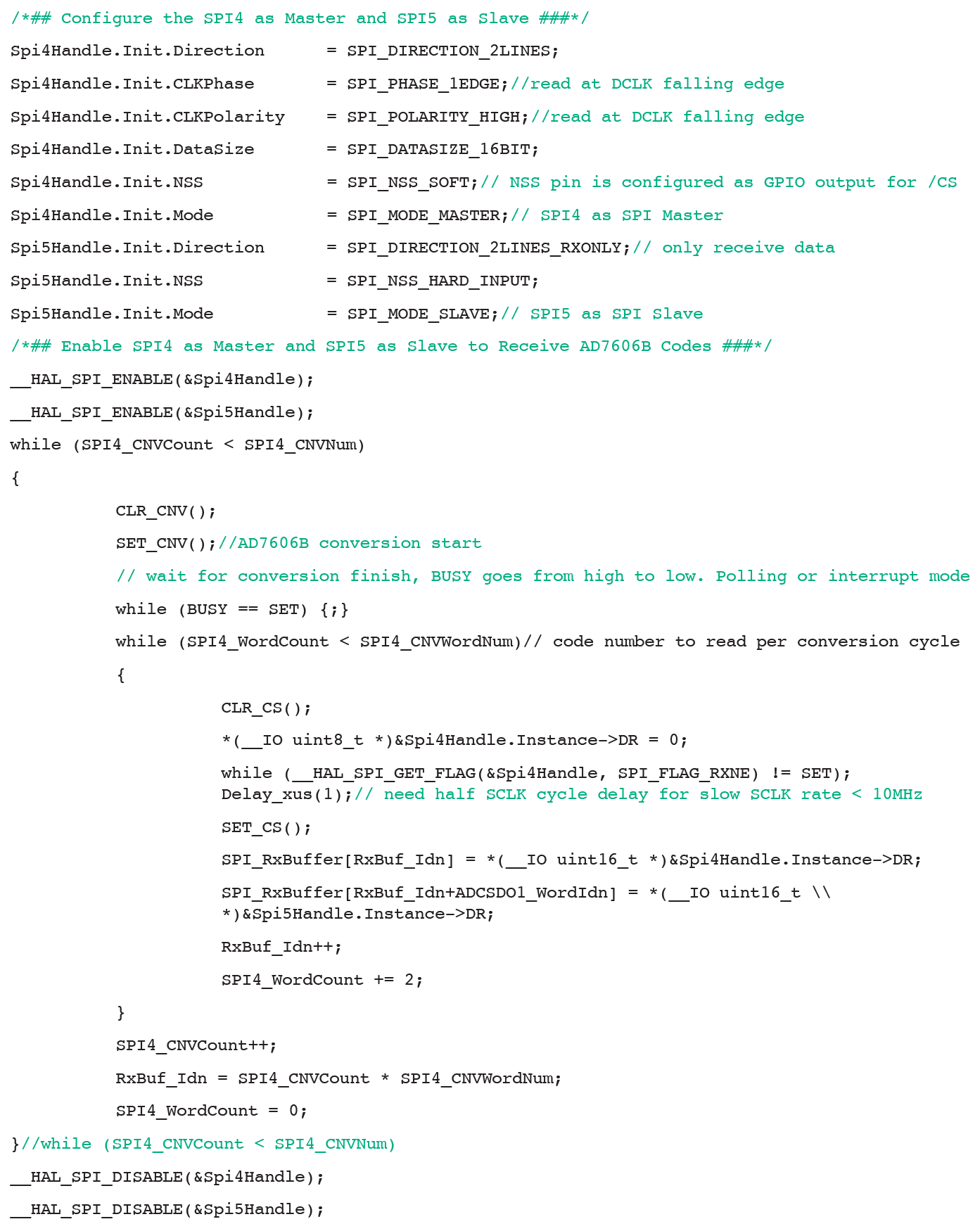
Figure 12. configures SPI4 as the master node and SPI5 as the node.
Figure 13 shows the digital interface capture of BUSY, SCLK, DOUTA, and DOUB for the AD7606B running at 240 kSPS.
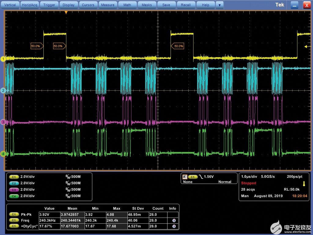
Figure 13. AD7606B busy, oscilloscope capture of SCLK, and data on DOUTA and DOUTB.
Conclusion
This paper has discussed methods for accessing ADCs with non-standard SPI interfaces using the microcontroller SPI. These methods can be used directly or with minor adjustments to control the ADC SPI, which can be used as the SPI main power supply or multiple DOUT lines for faster throughput rates.