The 80C51 internal RAM has 256 cells and is usually spatially divided into two areas.
The low 128 cells (00H~7FH) internal data RAM area and the high 128 cells (80H~0FFH) dedicated register SFR area.
Internal RAM low 128 cells
The 80C51 low 128 cells are the true internal data RAM area, a multi-functional multiplexed data memory, which can be divided into 3 areas by usage as shown in the following figure.
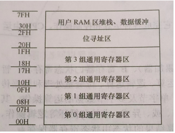
1) Working register area (00H~1FH)
Working register area is also called general-purpose register, there are 4 groups of registers in this area, each group consists of 8 registers, each cell is 8 bits, each group has R0~R7 as the register number, total 32 cells, the address of the cell is 00H~1FH.
At any moment, the CPU can only use one set of general-purpose registers, called the current general-purpose register group, which can be determined by the status combination of RS1, RS0 bits in the program status register PSW.
The general-purpose register bits provide the CPU with the convenience of accessing data in close proximity, increasing the working speed and providing convenience for programming.
2) Bit Addressing Area (20H~2FH)
The internal RAM has 16 cells from 20H to 2FH, counting 16*8=128 bits, with bit addresses from 00H to 7FH.
The bit addressable area can be used as a general RAM area for byte operation as well as bit operation for each bit of the cell, so it is called bit addressable area and is part of the storage space.
3) User RAM area (30H~7FH)
The remaining 80 cells are the user RAM area, the cell address is 30H~7FH, these cells can be used as a data buffer, in general applications set the stack in this area, the location of the top of the stack is indicated by the stack pointer SP.
A few notes on the use of internal RAM low 128 cells.
1>80C51 internal RAM 00H~7FH cells can be directly addressed or indirectly addressed to achieve data transfer;
2>The bit address space of internal RAM 20H~2FH can be used for bit operation, and the current working register group can be selected by software setting the status of RS1 and RS0 bits in PSW.
Internal RAM high 128 cells
The internal RAM high 128 cells are supplied to the dedicated registers, so they are called dedicated register area (also called special function register area, SFR area), and the cell addresses are 80H~0FFH.
The 80C51 has 22 special registers, of which the program counter is physically independent and has no address, so it is not addressable and it does not belong to the SFR area.
The remaining 21 special registers belong to the SFR area and are addressable. Their cell addresses are discrete from 80H to 0FFH, as shown in the table below.
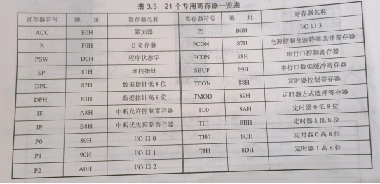
The following is a description of the dedicated register functions.
1) Program counter PC
PC is a 16-bit counter whose content is the address of the memory cell where the machine code of the instruction to be executed by the microcontroller is located, and it has the function of automatically adding 1 to realize the sequential execution of the program.
Since PC is not addressable, the user cannot read/write it, but can change its content by transfer, call, return, etc. The addressing range of PC is 64KB, i.e., the address space is 0000~0FFFFH.
2) Accumulator ACC or A
Accumulator ACC is an 8-bit register, which is the most commonly used special register with strong function and important status. It can store both operands and intermediate results of operations.
Many instructions in the 80C51 series microcontroller have operands from accumulator ACC. accumulator is very busy and is the bottleneck of microcontroller execution program, which restricts the improvement of microcontroller efficiency. now some microcontrollers have used register array to replace accumulator ACC.

3) Register B
Register B is an 8-bit register, mainly used for multiplication and division operations. When multiplying, the multiplier is stored in B. After multiplying, the high 8-bit result is stored in B register.
After the division operation, the remainder is stored in register B. Register B can also be used as a general register.
4) Program Status Word PSW
The program status word is an 8-bit register used to indicate the program running status information. Some of the bits are automatically set by the hardware according to the program execution result, while some bits can be set by the user through the instruction method.
The name and definition of each flag bit in PSW are as follows.
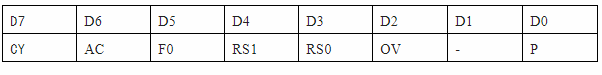
CY: The in (borrow) flag bit is also the bit accumulator of the bit processor C. In addition and subtraction operations, if the highest bit of the operation result has an in or a borrow bit, CY is automatically set to 1 by hardware, otherwise it is cleared to 0.
During bit operations, CY is used as accumulator C and participates in bit transfer, bitwise with, bitwise or bitwise operations. In addition, certain control transfer type instructions also affect the CY bit state.
AC: Auxiliary input (borrow) bit flag bit. In the addition and subtraction operation, this flag bit is automatically set to 1 by hardware when the lower 4 bits of the operation result are fed or borrowed to the higher 4 bits, otherwise it is cleared to 0.
F0: User flag bit, set by user through software to control program steering.
RS1, RS0: Register group selection bits. It is used to set the group number of the current general-purpose register group.
There are four groups of general-purpose register groups, and their correspondence is listed in the following table.
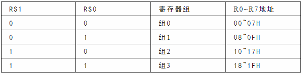
The status of RS1, RS0 is set by software, and the selected register group is the current general-purpose register group.
OV: Overflow flag bit, in addition and subtraction operation with signed numbers (complementary numbers), OV=1 means the result of addition and subtraction operation is beyond the 8-bit signed number representation range (-128~+127) of accumulator A, resulting in overflow, so the operation result is wrong. OV=0 means the result is not beyond 255, the result exists in A only.
When dividing, OV=1, means the divisor is 0. OV=0, means the divisor is not 0.
P: Parity flag bit, the parity status of the execution result containing 1, i.e. whether it is an odd number of 1 or an even number of 1.
5) Data pointer DPTR
Data pointer DPTR is a 16-bit register, it is the only one 16-bit register in 80C51. When programming, it can be used either as a 16-bit register or as two 8-bit registers separately.
DPH is the high 8-bit register of DPTR, and DPL is the low 8-bit register of DPTR. DPTR is usually used as an address pointer when accessing external data memory or I/O interface, and the addressing range is 64KB.
6) Stack Pointer SP
In the memory of microcomputers, there is a need to set up an area for last-in-first-out operation of data, which is called the stack.
The stack is usually part of the memory, in order to ensure that the data in the stack area can be operated according to the last-in-first-out rule, an address register is set up specifically to manage this address register called the stack pointer SP, which is used to indicate the address of the top unit of the stack.
The stack pointer SP is an 8-bit register in the 51 series microcontroller.
In 51 series microcontroller, when data is stored in the stack, the stack pointer will automatically add 1 and store the data in the memory cell pointed by the stack pointer. When data needs to be taken out from the stack, the data in the memory cell pointed by the stack pointer will be read out first, and then the stack pointer will be automatically subtracted by 1.
Therefore, the stack pointer always points to the unit in the stack where the data was last deposited, so it is called the top stack of the stack. Since the stack pointer automatically adds 1 (address increases) when data is deposited into the stack, it is called an up-growing stack.
The operation procedure: into the stack operation, first SP plus 1, after writing data; out of the stack operation, first read out the data, after the SP minus 1.
In the 51 series microcontroller, the stack is specified in the internal RAM of the microcontroller, while 81H is set as the stack pointer in the special function register, i.e. SP=81H, and the content of 81H indicates the top address of the stack.
The main function of the stack is to protect the breakpoint and protect the site. 51 series microcontroller system reset, SP = 07H.
Since the 89C51 has a limited on-chip RAM area, the smaller the top of the stack, the deeper the stack depth. In order to facilitate the use of all 4 groups of general-purpose register sets, the top of the stack is generally set at position 30H using MOV SP, #30H during system initialization.
There are two ways to use the stack, one is the automatic way, when calling a subroutine or interrupt, the return address is automatically put into the stack. In this way, no user action is required.
The other instruction mode, the in-stack instruction is PUSH and the out-stack instruction is POP.
7) Power control and baud rate selection control register PCON
PCON is an 8-bit register, mainly used to control the microcontroller working in low-power mode. 80C51 microcontroller has two low-power modes: standby mode and power-down protection mode.
The PCON register is not bit addressable, but only byte addressable.
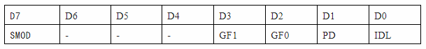
PD: Power down protection bit, when it is 1, it enters the power down protection mode;
IDL: standby mode bit, when it is 1, it enters standby mode.
8) Parallel I/O ports P0~P3
Dedicated registers P0, P1, P2, P3 are the data latches of parallel I/O ports P0~P3 respectively. In the 80C51 series microcontroller, there is no special I/O port operation instruction, but the same MOV instruction operation is used to use the I/O port as a general dedicated register.
9) Serial data buffer SBUF
The serial data buffer SBUF is a dedicated register for the serial port, consisting of a transmit buffer and a receive buffer. The two buffers are physically independent but share a common address (99H), and SBUF is used to store the data to be sent or received.
10) Timer/Counter dedicated registers
There are two 16-bit timer/counters T0 and T1 in 80C51 series microcontroller, they are composed of two independent 8-bit counters, T0 is composed of special registers TH0 and TL0, T1 is composed of special registers TH1 and TL1.
11) Control class special registers
IE, IP, TMOD, TCON, SCON registers are control registers for interrupt system, timer/counter, serial port, and contain control and status bits. The control bit is the control operation bit for programming write.
The byte addressing of the dedicated registers is explained in the following points.
1> 21 byte addressable dedicated registers are discrete and scattered in the high 128 cells of internal RAM, the rest of the free cells are reserved areas, undefined and not available to the user.
2>The program counter PC is the only dedicated register that cannot be addressed, PC does not occupy internal RAM cells, it is physically independent.
3>Only direct addressing method can be used for the dedicated registers, which can be written as register symbol or cell address form in the instruction.
Among the 21 addressable special registers, there are 11 registers whose byte addresses are divisible by 8 and can be bit-addressed, i.e., each bit of these special register cells can be bit-operated, and each bit has a fixed bit address.