With the reduction of signal rising edge time and signal frequency, electronic products EMI problems are increasingly concerned by electronic engineers, almost 60% of EMI problems can be solved by high-speed PCB. The following are nine rules.
Rule one: high-speed signal alignment shielding rules

In the high-speed PCB design, the clock and other critical high-speed signal lines, the alignment needs to be shielded processing, if not shielded or only partially shielded, will cause EMI leakage. It is recommended that shielded lines, every 1000 mil, punched holes to ground.
Rule two: high-speed signal alignment closed-loop rules

Due to the increasing density of the PCB board, many PCB LAYOUT engineers in the process of alignment, it is easy to make a mistake, that is, the clock signal and other high-speed signal network, in the multi-layer PCB alignment when the results of the closed loop, such a closed loop results will produce a loop antenna, increasing the radiation intensity of EMI.
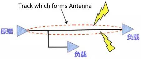
Rule three: high-speed signal alignment open-loop rules

Rule two mentions the high-speed signal closed loop will cause EMI radiation, however, open loop will also cause EMI radiation.
Clock signals and other high-speed signal network, in the multi-layer PCB alignment once the result of open loop, will produce a linear antenna, increasing the intensity of EMI radiation.
Rule four: the characteristic impedance of high-speed signals continuous rule
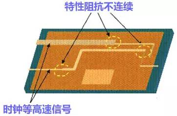
High-speed signals, switching between layers must ensure the continuity of the characteristic impedance, otherwise it will increase the EMI radiation. In other words, the width of the wiring of the same layer must be continuous, and the alignment impedance of different layers must be continuous.
Rule five: high-speed PCB design wiring direction rules
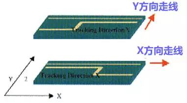
The alignment between two adjacent layers must follow the principle of vertical alignment, otherwise it will cause crosstalk between lines and increase EMI radiation.
In short, the adjacent wiring layers follow the horizontal and vertical wiring direction, vertical wiring can suppress crosstalk between lines.
Rule six: the topology rules in high-speed PCB design

In high-speed PCB design, the control of the characteristic impedance of the circuit board and the design of the topology in the case of multiple loads, directly determines the success or failure of the product.

The figure shows a daisy-chain topology, generally used in the case of a few Mhz for the benefit. High-speed PCB design is recommended to use the back-end star symmetric structure.
Rule Seven: Resonance rules for the length of the alignment
Check whether the length of the signal line and the frequency of the signal constitute resonance, that is, when the wiring length is an integer multiple of the signal wavelength 1/4, this wiring will produce resonance, and the resonance will radiate electromagnetic waves and generate interference.
Rule Eight: Return path rules

All high-speed signals must have a good return path. As much as possible to ensure that high-speed signals such as clocks have the smallest possible return path. Otherwise, it will greatly increase the radiation, and the size of the radiation and the signal path and the area surrounded by the return path is proportional.
Rule nine: the device decoupling capacitor placement rules

The placement of decoupling capacitors is very important. The placement is not reasonable at all to achieve the decoupling effect. The principle is: close to the power supply pins, and the capacitor’s power supply alignment and ground surrounded by the smallest area.