FPGA project development of synchronous signals and sub-stable
Let’s start with flip-flops, all of which have a set-up TIme and hold TIme window around the active clock edge, during which the data must not change.
If the data in this window actually changes, the output of the flip-flop will go into an indeterminate state, which is neither a logic 0 nor a logic 1. After a defined recovery TIme, the flip-flop output will revert to a logic 0 or a logic 1.
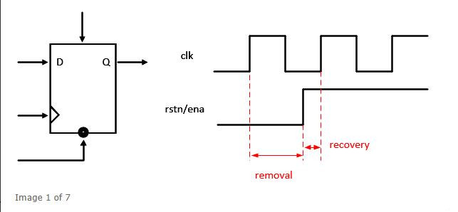
The build and hold times and recovery times are unique for each family of devices, and this information is typically defined in the datasheet or application note. In general, when we design FPGAs to meet timing constraints, we don’t have to worry too much about them because Vivado will try to meet the performance defined in the constraints.

However, when we have asynchronous signals coming into the FPGA or multiple clock domains that are asynchronous to each other, we need to think carefully about the design to ensure that we do not violate the build and hold times and cause sub-stability. Of course, in either case, we can’t prevent a sub-stable event from occurring, but we can ensure that our design doesn’t have incorrect data as a result of a sub-stable event.
Of course, one obvious case is that the input signal is asynchronous to the internal clock, and the composition in the same clock domain is not yet well understood. We can use some simple rules; if the clock is an integer division of the common clock, we are in the same clock domain. If the clocks are non-integer divisors, they are not in the same clock domain, or come from different sources (even if they have the same clock frequency)
There are several designs to choose from when synchronizing signals to the FPGA or to a different clock domain. In xilinx fpga, the best way to do this is to use xilinx parameterized macros that are created to solve CDC / SynchronizaTIon problems. xPM provides a range of macros, including
Single Static Synchroniser (Single Static Synchroniser) – the classic single-bit flip-flop synchroniser
Pulse Data Synchroniser – transferring pulses from one domain to the next
Data Bus – multiplexer, FIFO, handshaking and Gray Code based transfers
In Vivado, we now easily implement XPM structures in IP Integrator to make CDC crossing visible.

Careful consideration needs to be given to which structure to use. For example, do not attempt to synchronize multiple data bits using a single bit synchronizer, as there is no guarantee that the transmitted data will be aligned, leading to data corruption. Attention also needs to be paid to recombination, which is where two or more static signals span the clock domain and recombine in the logic function. Delays in the synchronizer can cause downstream logic to be affected due to sub-stable recovery.
Despite our best efforts to mitigate CDC in our designs, we are human and we make mistakes, so we can use the built-in Vivado option to report CDCs that occur in our designs.
Once synthesis is complete, we can run the CDC report without waiting for place and root to complete.
Run the command report_cdc from the TCL console – there are many options for writing out files, analyzing specific paths, or creating exemptions.

This will show all clock domain crossings in the design and if there are any unsafe or unknown crossings. In the example above, you can see that there are 6 unsafe and several unknown. If we run the command with the option -details, we will see all the paths reported. Clicking on an unsafe or unknown path will open the path of interest for us to check.
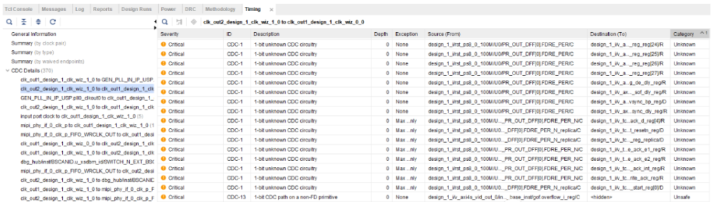
After selecting the path, we can open the schematic viewer of the path we are interested in. The problem in this case is that the reset is generated by a different clock.

Knowing this, we can correct the problem by updating the design, e.g., correcting errors, inserting necessary synchronization structures, or correcting constraints to update the path.

FPGA Project Development for 7 Series FPGAs Advanced SelectIO Logic Resources

Clock Planning for FPGA Project Development