Spin Transfer Torque Magnetoresistive Random Access Memory (STT-MRAM) is a persistent storage technology that provides performance, persistence and endurance using a variety of industry standard interfaces.
Everspin has introduced the STT-MRAM product, which leverages a variant of the JEDEC standard DDR4 interface known as JE-DDR4, which includes unique features needed for complete system support. This article will help engineers understand the Everspin STT-DDR4 design guide for Xilinx FPGA controllers

Enabling ST-DDR4
To enable designers to quickly integrate ST-DDR4 support, the process begins with the existing 8Gb DDR4 SDRAM-2666 Memory Interface Generator (MIG) generated in the Xilinx Vivado development environment. The differences from 8Gb DDR4 SDRAM are as follows and will be described in subsequent sections.
- Timing (reduced operating frequency, increased line access time, increased counter width and reduced CAS page size)
- Power-up (calibration – anti-smear mode is enabled during calibration)
- Power down (stuff or move all relevant data to persistent memory arrays)
- performance (increase pipeline depth and improve data transfer efficiency)
Note: Robust ST-DDR4 persistent memory designs also require a system-level error correction code (ECC) scheme, but that document is outside the scope of this document.
DDR4 SDRAM-1333 Memory Interface
In the Xilinx design environment, DDR4 interface logic will be generated based on input parameters representing the speed and timing characteristics of the 8Gb SDRAM DDR4-2666.

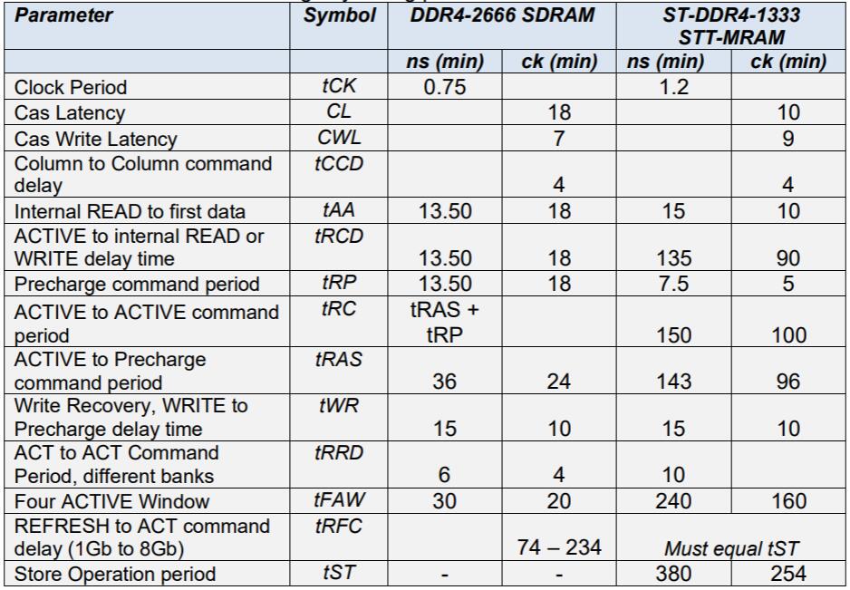
This table shows the key timing parameters for DDR4 and ST-DDR4
Since MIG cannot create interface logic using parameters outside of the current JEDEC standard, a JEDEC-compatible DDR4 controller must first be created.
The everspin 1Gb ST-DDR4 1333 device is most similar to the 8Gb DDR4-2666 SDRAM device, so please use the timing values from the 8Gb DDR4 SDRAM 2666 specification SDRAM DDR4-2666. Once the DDR4 interface logic is created, the timing, power-up, power-down and performance parameters can be modified to enable ST-DDR4 persistent memory.
It is highly recommended to create an example test bench in Vivado after creating the MIG by right-clicking on the .xci file and selecting the menu item named ” Open IP Example Design …”. menu item. Creating an example design will create a new Vivado project. and all the test files needed to simulate the newly created MIG.
