Nowadays, server physical machines are usually multiple CPUs and have dozens or even tens of cores. The memory is tens of GB or even hundreds of gigabytes, and is also composed of many strips. So let me think about this: How are so many CPUs and memory connected to each other? Does the same CPU core access different memory sticks with the same latency?
In “Memory Random Access is also Slower than Sequential, Taking You Deeper into the Memory IO Process” we learned about the execution process inside the chip during memory access, and in “Actual Testing of the Access Latency Difference between Sequential IO and Random IO in Memory” we conducted an actual code test. However, in both articles we focused on the internal memory mechanism and avoided the above issue, which is the way the CPU and memory are connected, that is, the bus architecture

1 Reviewing the simple connection between CPU and memory: the FSB era
Let’s review the FSB bus solution in the days when the number of CPUs and memory was relatively small, the full name of the FSB is Front Side Bus, so it is also called the Front Side Bus, and the CPU is connected to the North Bridge chip through the FSB bus and then to the memory. The memory controller is integrated into the North Bridge, and all communication between the Cpu and the memory is carried out through this FSB bus.

In this era, the way to improve the overall performance of computer systems at that time was to continuously increase the data transfer frequency of CPUs, FSB buses, and memory sticks.
2 Today’s complex interconnection of multiple CPUs and multiple memories: the NUMA era
When the CPU main frequency was increased to 3GHz per second, hardware manufacturers found that individual CPUs had reached their physical limits. So they changed the method of performance improvement to multi-core, or even multi-CPU direction. In this case, if the FSB bus was still used, it would cause all CPU and memory communication to go through the bus, which would become a bottleneck and prevent the full advantage and performance of multi-core. So CPU manufacturers have moved the memory controller from the Northbridge to inside the CPU so that the CPU can communicate directly with its own memory. So what if the CPU wants to access memory sticks that are not directly connected to itself? So a new bus type was born, and it is called the QPI bus.

In Figure 2, CPU1 needs to go through the QPS bus if it wants to access memory 3.
3 Getting hands-on with the NUMA architecture under Linux
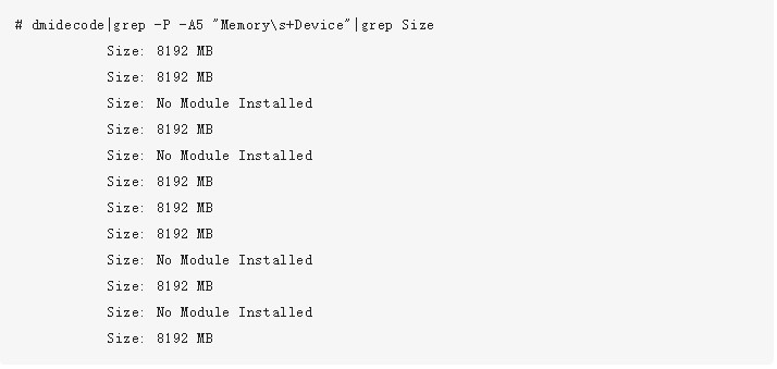
Let’s start by looking at the memory slots, individual sizes, and other information with the dmidecode command. You can try to execute the following command on linux. The output is very long, so you can study it carefully sometime. I will not cover all of them here, but just pick some memory related ones here.
2、Let the memory and CPU in different Node
The following code may need to slide left and right

5 Conclusion
As we can see from the above subsections, modern servers have multiple CPUs and memory sticks, which are currently interconnected mainly using the complex NUMA architecture, which divides the CPUs and memory groups in the server into different nodes. from the above experimental results, taking a case with an 8M array and a loop step size of 64, the same node takes 3.15 nanoseconds and 3.96 nanoseconds across nodes. So it is faster to access between CPU and memory belonging to the same node. And if it crosses node, it needs to go through QPI bus, and overall, it will be slightly slower.
Reviewed and edited by Qing Liu