The need for flexible timing solutions in circuit boards and associated devices triggered a need for clock buffers. As one of the broader components of clock trees, the buffers help to create variations of the original (reference) clock, thereby, helping in the distribution of the timing solutions across all facets.
In this article, we are going to introduce you to what a clock buffer is, including some of the major features and the best ones out there.
How does a Clock Buffer Work?
A clock buffer works by creating the derivatives, variants or copies of the clock, which it is referencing. In most cases, the reference clock is either the Crystal Oscillator (XO) or a Clock Generator.
Whichever of the two that is used, the goal is to help make more copies of those referenced clock.
Why, you may ask? The reason is this: when a clock buffer makes copies of the reference clock, it helps to scale the outputs, as well as create a more distributive pathway for these outputs.
When to Use a Clock Buffer
There may be no need for a clock buffer, and that is because the requirements aren’t there in the first place.
If you must use a clock buffer in your target device, it must be based on the target device. Typically, the target device or application must have required the same signal. By using the clock buffer, it creates multiple pathways for the outputs, which would then be subject to an onward distribution to the multiple targets.
Top Clock Buffers to Buy
Now that you know that the clock buffer is important for the target devices or applications, what options do you have?
Here are the top seven (7) clock buffers you can find in the market and how they work:
1. PI6C49CB01Q2WEX
This is Diodes Incorporated’s Clock Buffer. Designed as a 1-to-1 Differential-to LVCMOS/LVTTL Translator High Performance Buffer. It is based on the automotive AEC-Q100 rating and is ideal for applications (devices) with a smaller footprint (board space).
The following are some of the properties:
- Operating Temperature of -40-degree Celsius to 85-degree Celsius for both the Automotive Grade 2 and the Automotive Grade 3 temperature ranges.
- A maximum part-to-part skew of 500ps.
- It uses a LVCMOS/LVTTL output.
- PI6C49CB01Q2WEX maintains an ambient operating temperature of -40-degree Celsius to 105-degree Celsius.
2. 8SLVP1204ANLGI
8SLVP1204ANLGI is a multiplexer, low-phase noise, fanout buffer, designed for excellent distribution of signals. The major characteristics are:
Easy Interfacing of Single-Ended Signals
With the focus on signal distribution, 8SLVP1204ANLGI ensures that its interface is optimized for the same. For example, the integrated bias voltage reference enables the interfacing or the connection of the single-ended signals to the input ports of the target devices.
Flexible Power Supply
8SLVP1204ANLGI’s power supply is flexible. It interfaces from either the 2.5-volt power supply or the 3.3-volt power supply interface.
Optimized for the Lowest Performance Requirements
By default, clock buffers are designed to channel signals across the required pathways, while using the lowest resources.
8SLVP1204ANLGI uses low additive phase noise and low power consumption.
The additional features are:
- Between -40-degree Celsius and 85-degree Celsius of operating temperature.
- It supports the following inputs: LVPECL, CML and LVDS.
- Supports only one circuit.
- Voltage Supply: 2.375V to 3.63V
- 8SLVP1204ANLGI uses LVPECL as the output.
- 2 Gigahertz (GHz) as the maximum frequency.
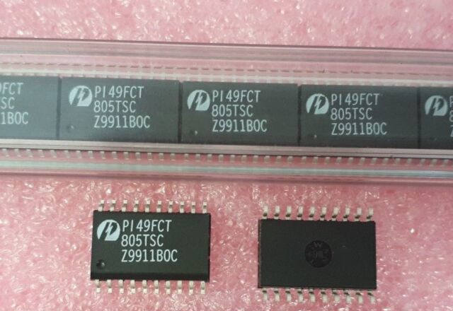
3. PI49FCT3803LEX

PI49FCT3803LEX is a 1:7 clock buffer, specially optimized for network applications. It uses up to 3.3-volt supply voltage and has up to 70-degree Celsius as the operating temperature.
The additional features are:
- High Frequency: It supports up to 156 MHz operating frequency.
- PI49FCT3803LEX has a low propagation delay of 2.6 nanoseconds (ns).
- Tolerant Input of 5V
- It supports a 3.3V supply voltage.
Clock Distribution for Synchronous Systems
PI49FCT3803LEX provides an excellent clock distribution for the synchronous systems. It does this via the low-skew of 250ps, between any of the two output clocks.
Worthy of noting is that the support for synchronous systems is in line with the buffer’s low-skew, low jitter and high-frequency clock distribution.
4. NB3N2304NZDTR2G
NB3N2304NZDTR2G is a 1-to-4 clock fanout buffer with low skew capabilities and supports between 3 volts and 3.6 volts of voltage (supply).
NB3N2304NZDTR2G is designed for the high-speed clock distributions, especially for the PCI-X-centric applications.
Here are some of its additional properties:
Output Enable (OE)
The Output Enable (OE) feature on the NB3N2304NZDTR2G is designed to balance the outputs, by forcing the outputs LOW when LOW.
Optimal Layout
The optimal layout and design of the NB3N2304NZDTR2G clock buffers helps in the minimization of skews, especially when these skews are to be used either for device-to-device or for standalone purposes.
NB3N2304NZDTR2G uses an industrial temperature range and is packed in an 8-pin TSSOP, measuring 4.4mm by 3mm.
Target Applications
It is best to use the NB3N2304NZDTR2G clock buffer for either the networking clocks or the PCI-X applications. It is also better to use it with applications requiring low output-to-output skew.
5. PL133-27GI-R
Small form-factor or compact applications/devices deserve to also maximize the potentials of a clock buffer. The PL133-27GI-R has been specially manufactured for such devices. It is an advanced inverting fanout clock buffer, designed for the small form-factor and high-performing applications.
One of the buffer’s highlights is the offering of the best jitter performance, lower power consumption and phase noise for these applications.
It will also be of interest to you to know that the PL133-27GI-R also supports a reference clock of between 1 Megahertz (MHz) to 150 Megahertz (MH). This support is in place to aid the production of two circuit outputs of the same frequency.
Looking for more reasons to invest in the PL133-27GI-R clock buffer? Here are some more:
Varied Operating Temperature Ranges
The buffer’s operating temperature ranges are between 0˚C and 70˚C for the commercial use cases and between -40˚C and +85˚C for the industrial applications.
6. LTC6957IMS-3#TRPBF
Analog Devices Inc., one of the major producers of semiconductor devices, manufactured the LTC6957IMS-3#TRPBF clock buffer.
The company aimed at using this clock buffer to create a clock fanout buffer distribution method for the channeling of signals to the right pathways.
This is no doubt, one of the best clock buffers you will work with, not just because of the multiple outputs but also because of the 1:2 input to output ratio.
Here are some of the things you need to know about the clock buffer:
Low Phase Noise
No doubt, when a clock buffer or any of the other important semiconductor components is in use, they tend to make a lot of noise. That doesn’t appear to be the case with the LTC6957IMS-3#TRPBF, thanks to its low phase noise design.
The delivery of the lowest possible phase noise signal is because of the maximum contributions of the input stage filtering and noise limiting function.
By delegating this function, the LTC6957IMS-3#TRPBF clock buffer is now able to operate at the same noise level as the sine wave system reference – which is about 10MHz.
Multiple Input and Output Levels
Generally, the family of LTC6957 clock buffers, of which the LTC6957IMS-3#TRPBF belongs to, is known for the use of multiple input and output levels. The input signals can either be any logic level or a sine wave.
The output levels of the LTC6957 clock buffers typically include CMOS, LVPECL and LVDS. In the case of the LTC6957IMS-3#TRPBF, it uses the CMOS as the output level and a combination of LVDS, CML, LVPECL and CMOS as the input levels.
Logic Converter
Without letting any of the logics to waste, the LTC6957IMS-3#TRPBF uses a logic converter to make the most out of those.
For example, the LTC6957IMS-3#TRPBF has an optimized conversion of the sine wave signals into the corresponding logic levels.
Ideal for High-Frequency Applications
LTC6957IMS-3#TRPBF is ideal for the applications requiring a higher frequency. Examples of these applications are:
- High-speed data acquisition
- System reference frequency distribution
- Test and measurement
- Military and secure radio
- Medical imaging
- Low noise timing trigger
- High-speed DDS Clock Driver, ADC and DAC.
- Broadband Wireless Transceiver
7. PI6CB33601ZLAIEX
PI6CB33601ZLAIEX is a low-power, 6-output PCIe Gen1 to Gen5 clock buffer. Designed to promote clock buffering with on-chip termination, it helps to make layout mapping easier, balances power management and can potentially save up to 24 external resistors.
Optimized Circuit Board Performance
PI6CB33601ZLAIEX is ideal for circuit boards with optimized performance requirements. This, it delivers via the SMBUS that delivers a combined function of amplitude and slew rate. The two helps in the further optimization of the individual circuit boards.
The following are some of the PI6CB33601ZLAIEX’s additional features:
- Low jitter outputs
- Spread spectrum tolerance
- Up to 3.3-volt supply voltage
- Less than 50ps of differential output-to-output skew.
- It supports up to 6 differential low-power HCSL outputs with on-chip termination.
8. SY75604BTWL-TR
Microchip Technology’s SY75604BTWL-TR clock buffer delivers a wide range of voltage performances, including the support for the 1.62, 1.9, 2.25 and the 3.63 volts.
It uses both the HCSL for the input and output and can balance the functions perfectly with the 1:4 input-to-output ratio.
As for the package, it uses the 16-VFQFN package with an exposed pad. The exposed pad doubles as a heatsink of sorts; helping in the removal of (excessive) thermal energy from the buffer.
Both the operating temperature and the operating frequency are impressive, clocking up to 105-degree Celsius and 250 Megahertz (MHz), respectively.
9. MC100LVEP14DTG
onsemi’s MC100LVEP14DTG is a 1:5 differential clock driver, supporting the applications with HCSL inputs and which can be used when operating under the PECL conditions.
Common Enable Function
The Common Enable (EN) function on the MC100LVEP14DTG is synchronous and the outputs are either disabled or enabled when operating in the LOW state.
Unlike the asynchronous control that tends to have a runt clock pulse, the synchronous control on the MC100LVEP14DTG doesn’t have that. In its place is the clocking of the internal flip flop on the falling edge of the input clock. Doing this ensures that the associated specification limits are referred to the negative edge of the input clock.
Support for Input Multiplexer
MC100LVEP14DTG supports input multiplexer because of the acceptance of two clock sources.
These dual clocking sources help the clock buffer’s drive for excellent clocking distribution on the target applications.
10. NB3N551DG
NB3N551DG is also from onsemi’s stable, but this time, it is used to provide a 1-to-4 input-to-output clock fanout buffer ratio, designed to aid the transition from low output-to-output skewing.
The hallmark of its design is the use of the Surface Mount Technology (SMT) to enable the minimized skew processing, optimal layout and flexible design within a device or across multiple devices.
Choosing a Clock Buffer: Factors worth Considering
No doubt, using a clock buffer goes a long way to facilitate the distribution of multiple copies of a major clocking interface to the other Integrated Circuits (ICs) on the board that rely on the same frequency requirements.
No matter where the copies are generated from, the goal is to maximize them to create sustainable paths for the onward transmission of the frequencies to the designated paths.
To that end, your choice of a clock buffer, especially from the list we made should be based on the input frequency division, the level of translating the signals and whether the buffer supports multiplexing.
Understanding the Difference between a Clock Buffer and a Regular Buffer
If you are looking to buy a clock buffer, there is also a chance that you want to compare the options before you. Clock buffers are typically compared to the regular or traditional buffers.
We want to highlight some of the key differences between the two.
Minimum Rise and Fall Time
It is peculiar to see the regular buffers use an irregular (minimum) rise and fall time. It is common because the rise and fall time is driven by the W/L ratio.
On the other hand, the Clock Buffer uses a balanced/equal rise and fall time, which helps in perfecting the signal transmission. Besides, the balanced rise and fall time prevents the inordinate changes in the clock’s duty cycle signal.
Conclusion
Don’t forget to consult a professional clock buffer specialist to clarify you further on the things you need to know before you invest in one.