In an oversampling ADC, a very effective way to increase SNR is to increase the sampling rate to increase the oversampling rate. This requires a higher bandwidth for the integrator and op-amp, which results in higher power consumption, provided that all other devices remain unchanged.
Using the double sampling technique, the following can be achieved.
the clock frequency can be reduced to half its original size while maintaining the original OSR, thus doubling the time required for the op-amp build-up and resulting in lower op-amp power consumption

While keeping the op-amp and sampling frequency unchanged, the effective sampling frequency is doubled and the OSR doubled, resulting in a better noise shaping effect.
Introduction to the principle of the double sampling integrator
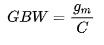
The commonly used op-amp gain bandwidth product GBW can be expressed as equation (1).
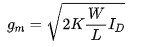
The relationship between gm and current can be expressed as Eq. (2)
For a normal switched-capacitor integrator, doubling the sampling clock frequency requires doubling the GBW and therefore increasing the operating current by a factor of four if the width-to-length ratio of the op-amp input pair is kept constant.
However, for a normal switched-capacitor integrator, the op-amp is idle when the clock is in the input sampling phase. By using two sampling capacitors operating at interleaved clocks, the op-amp can be used more efficiently and the input signal sampled at double the frequency. This is the basic idea of double sampling.
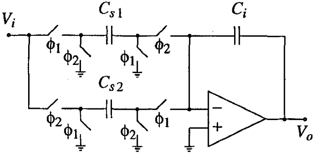
Picture
Figure 1 Single-ended implementation of a double-sampling integrator
Figure 1 shows a single-ended implementation of a double-sampling integrator. In this circuit, the input signal is sampled by two different capacitors, capacitor CS1 is sampled in phase Φ1 and integrated in phase Φ2, and capacitor CS2 is sampled in phase Φ2 and integrated in phase Φ1. Thus, both sampling and integration exist simultaneously in both phases of the clock, and the effective sampling frequency thus becomes twice as high.
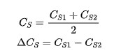
Disregarding other non-ideal factors, the transfer function of the double sampling integrator can be expressed as equation (3)
where
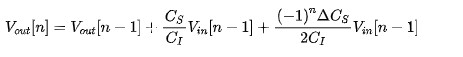
n=0 occurs when Φ2 is high, also note that n stands for the nth valid sample period, not the sample clock period! Double sampling allows for two valid sample periods in each sample clock cycle.
The left two terms of equation (3) are an ideal delay integrator, but the last term is the product of the input signal and (-1)n. This characterises the signal obtained when a cosine signal with a frequency half the sampling frequency (fs/2, i.e. the clock frequency fc) is sampled and modulated with the input signal, which is caused by the mismatch between the two sampling capacitors.
For the input signal sampling, the above modulated signal does not appear in the signal band due to the very low frequency of the input signal and therefore does not affect the input signal.
However, for the modulator’s feedback DAC, since the DAC output contains high frequency quantization noise, the mismatch causes the above signal modulation phenomenon to fold the quantization noise back into the band, thus worsening the modulator’s SNR. this phenomenon is the main drawback of the double-sampling Sigma-Delta modulator!
Several solutions to this problem are commonly used, including the design of the integrator circuit structure to offset the extra charge transfer generated by the mismatch, the placement of the NTF zero at fs/2, the use of a single capacitor for the DAC, etc. The interested reader is referred to the relevant literature.
Summary
This paper has briefly introduced the starting point and basic principles of the double sampling technique, and its main drawbacks at present. We hope that the reader will correct us.