PCIE Introduction
PCI Express is a high-speed interface bus used to interconnect computers and peripheral devices. It is a bus that can be used in mobile devices, desktop computers, workstations, servers, embedded computers and communication platforms.
PCIe can achieve point-to-point communication serial communication between two devices, if multiple devices need to be interconnected through a switch (Switch), so that a system can be connected to multiple devices.
The PCIe bus serves as a local bus for the processor system, and its role is similar to that of the PCI bus. The main purpose is to connect external devices in the processor system, but of course the PCIe bus can also be connected to other processor systems. The PCIe architecture is implemented in a slightly different way in different processor systems. However, in most processor systems, the basic modules RC, Switch and PCIe-to-PCI bridge are used to connect PCIe and PCI devices. In the PCIe bus, the devices based on the PCIe bus, also known as EP (Endpoint).

In computer communication platforms , PCI Express architecture represents a high-performance method of interconnecting peripheral components
1, evolved from PCI and PCI-X architecturearchitectures
- PCI Express interconnects two devices in a serial, point-to-point fashion
- Information transfer is implemented based on packet protocols
4, PCI Express interconnection can be achieved in a single channel or multi-channel data transfer
5, PCI Express protocol has been released in four versions

The characteristics of PCIE are as follows.
1、 Point-to-point transmission
2、 Serial bus means less pins are used
- Number of channels can be selected: x1, x2, x4, x8, x12, x16, x32
4, Full duplex communication
5、 2.5Gbps / 5.0Gbps
6、 Packet-based transmission protocol
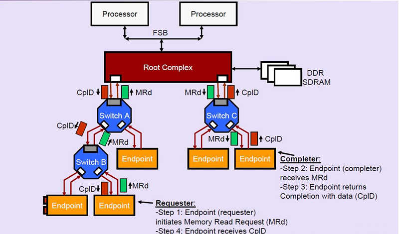
The application architecture of PCIe in computer architecture is as follows.

From the above we can see that the PCIE application architecture consists of four main parts.
1, FSB bus CPU interaction bus: FSB bus (Front Side Bus) is the CPU and DDR memory interaction bus
2, Root Complex: RC (Root complex) is an important structural component of the PCIe architecture system, RC proposed and X86 system architecture is closely related, in fact, only in the x86 architecture there is a standard RC specification definition, while in other systems there is no standard definition of the full function of the RC. For example, the X86 architecture contains DDR controller and FSB to PCIe bridge, while the ZynqSoc chip architecture contains AXI to PCIe bridge and DDR controller, and PowerPc only contains a PCIe bus controller. Here we need to pay attention to the Root complex including the root port.
3, PCIe Switch: Switch PCIe link through the Switch for link expansion
4, PCIe End point: that is, the common PCIE terminal device, FPGA most commonly used is also End point.
FPGA in PCIE can become Root Complex, Switch and End point.
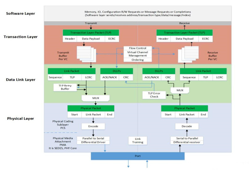
The PCIe bus hierarchy consists of three main layers, mainly the transaction layer, the data link layer, and the physical layer.
- Transaction layer: The highest layer of the PCIe bus hierarchy, which receives data requests from the core layer of PCIe devices and converts them into PCIe bus transactions, and these bus transactions used by the PCIe bus are defined in the TLP header.
(Explanation: The main meaning is that the transaction layer encapsulates the data into TLP packets and sends them to the lower layers)
- Data Link Layer: TLPs are sent to the physical layer after passing through the data link layer with a Sequence Number prefix and CRC suffix.
3, physical layer: PCIe electrical characteristics, circuitry, etc. Before the PCIe link can work properly, link training is needed for the PCIe link, and in this process, it is used.
LTSSM state machine. the full name of LTSSM is Link Training and Status State Machine. this state machine is in the physical layer of PCIe bus. The state transfer diagram is as follows.
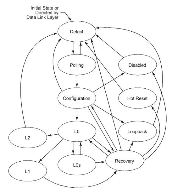
The Detect state is the beginning of the PCIe link training. In addition, Detect, as the name implies, needs to be implemented to detect the work. Because in this state, the transmitter TX needs to detect whether the receiver RX exists and can work properly, if the detection is normal, then it can enter other states. The logic to determine the presence of RX is relatively simple, it is through a “Detect logic” circuit to compare the size of the RC time constant.

From the above figure, you can find that the time constant becomes larger when the PCIe terminal is connected. This is how we decide whether the Detect state will go to the next state or not.
The purpose of the Polling state is to “code” and achieve unobstructed communication. After entering this state, the TX and RX send TS1 and TS2 OS sequences to determine Bit Lock, Symbol Lock, and resolve Lane polarity reversal.
Bit Lock: During Bit transfer, the RX PLL locks the TX Clock frequency, a process called “Bit Lock” for RX.
Symbol Lock: The RX side of the serial to parallel converter knows how to distinguish a valid 10-bit Symbol, this process is called “Symbol Lock”. The COM control character is used here. (Explanation: also known as frame synchronization)

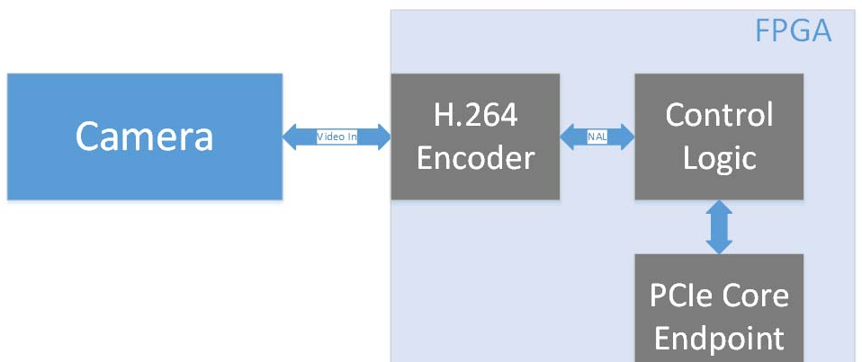
Common video programs are as follows.
Implementation of PCIE in FPGAs.
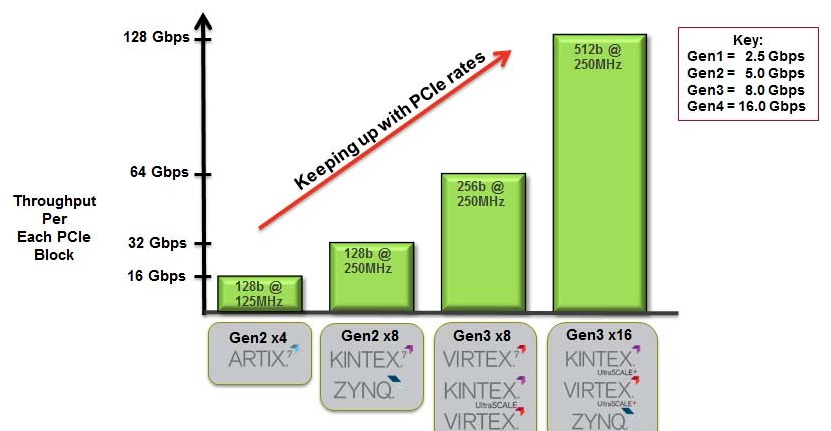
1, 7 series FPGAs support the implementation of Gen1 and Gen2 PCIE protocols
2、Virtex-7 FPGAs support the implementation of Gen3 PCIE protocol
3、UltraScale and UltraScale+ support Gen3 PCIE protocol
4, support x1, x2, x4, x8, x16lanes path
5, PCIE’s hard core uses the GTP interface for serial data transfer
The speed transfer rate of PCIE is as follows.
The overall block diagram for the introduction of PCIE hard cores in FPGAs is as follows.
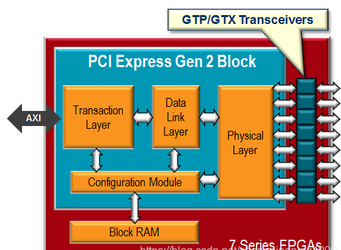
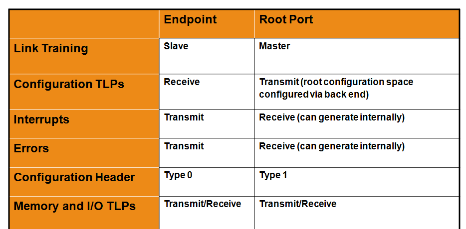
1、The hard-core PCIE supports Endpoint and Root Port
- Support AXI4-Stream user interfaces.
x1, x2, x4, and x8 lanes; 64-bit and 128-bit bit widths
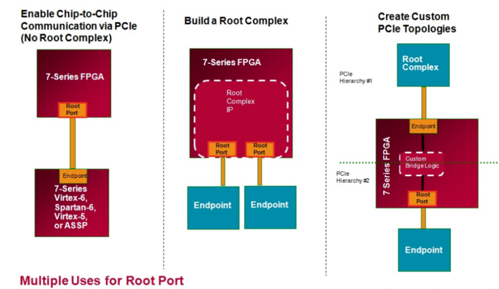
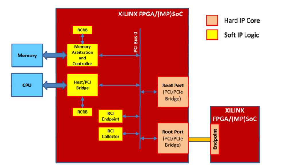
Root Port Overview
Xilinx FPGAs support hard-core root ports, but not hard-core root complexes. root complexes include one or more root ports, memory, IO subsystems, etc. root ports are simply ports provided for switch or endpoint connections. The relationship between the two is as follows.
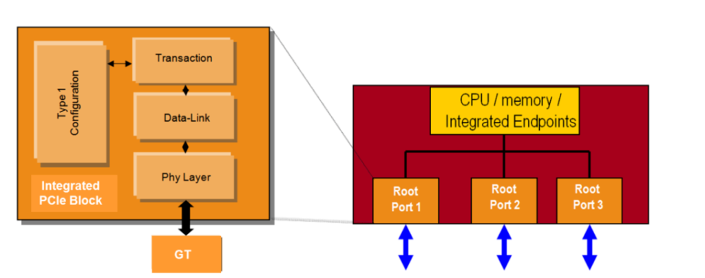
The root port is often used in simple designs, such as connecting to a single endpoint. root complexes have supporting software environments and complex designs.
Common examples of FPGAs building root ports are as follows.
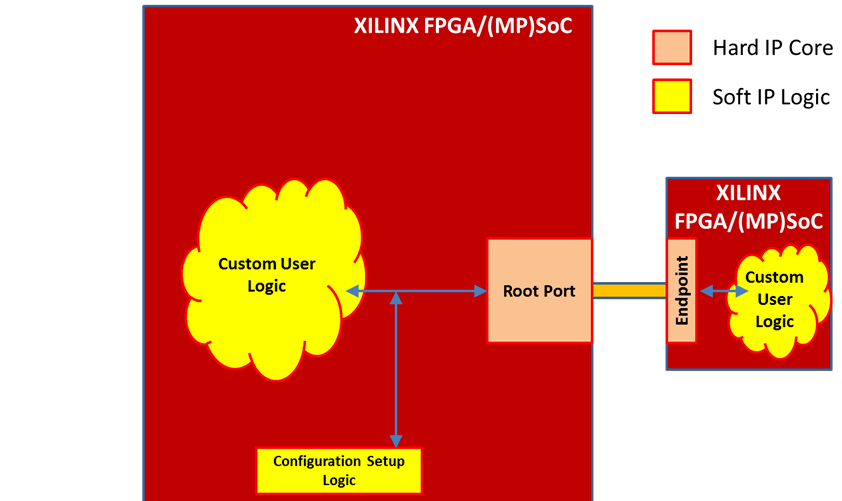
Common examples of FPGAs building root complexes are as follows.
There are also many differences between root ports and endpoints. root ports use Type 1 configuration headers. endpoints use Type 0 configuration headers. The main differences between the two are as follows.
Brief description of PCIE protocol
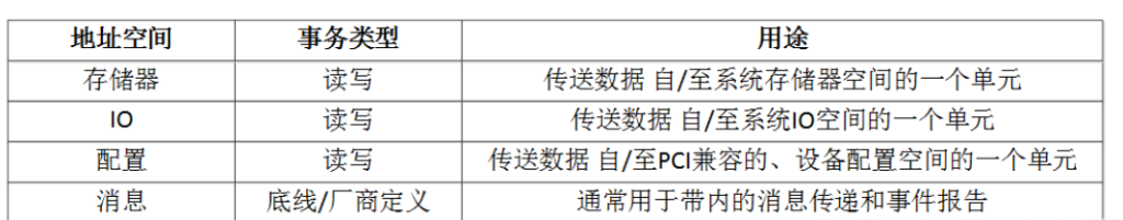
Address Space of PCIE
PCI Express implements four types of address spaces.
- PCIe configuration space (up to 4KB)
- Required, each PCI device has its own configuration space mapped to memory
- The first 256 bytes are PCI-compatible
- PCIe memory mapping space
- Optional, according to the device function to choose whether to map the memory space
3、 PCIe IO mapping space
- Optional
4、 PCIe message space
Among them, PCIe message space is mainly used for the use of interrupts, memory mapping space is used for the transfer of large amount of data, and IO mapping space is used for the transfer of small amount of data.
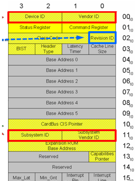
Type0.
- Used to configure endpoint devices
- Initiated by the root complex to configure a predefined PCI system endpoint device header area
- Device number/ID number
- BAR
Type1 type.
- Used to configure Switches/Bridges/end points
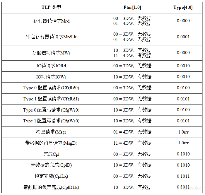
PCIE TLP packet data types
The above has explained that PCIE includes transaction layer, data link layer, and physical layer respectively, and the role of each layer for TLP packets is as follows.

The 3DW and 4DW here are actually tied to whether the address is 32 or 64 bits.
The specific TLP packets at each protocol layer are as follows.
The types of TLP packages in PCIE are as follows.

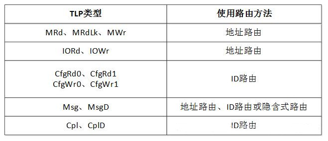
PCIE’s routing types
Each request or completion message header of PCIE is marked with a type, and the routing of each packet is based on the following three ways:
1、 Address routing
2、 ID routing
3、 Implicit routing
Endpoint address routing
The endpoint device checks the address in the TLP packet and compares it with all addresses in the BAR, and rejects it if it does not fall within the scope of this endpoint.
ID routing of the endpoint
The endpoint device checks the Bus ID and Device ID function IDs in the TLP packet for consistency with this endpoint, and this information is captured in the configuration information for Type0.
The different types of TLP packets correspond to the routing types as follows.
PCIE point-to-point transmission block diagram
- Configure IO transfer
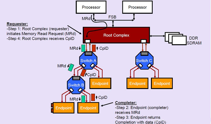
2、DMA transfer
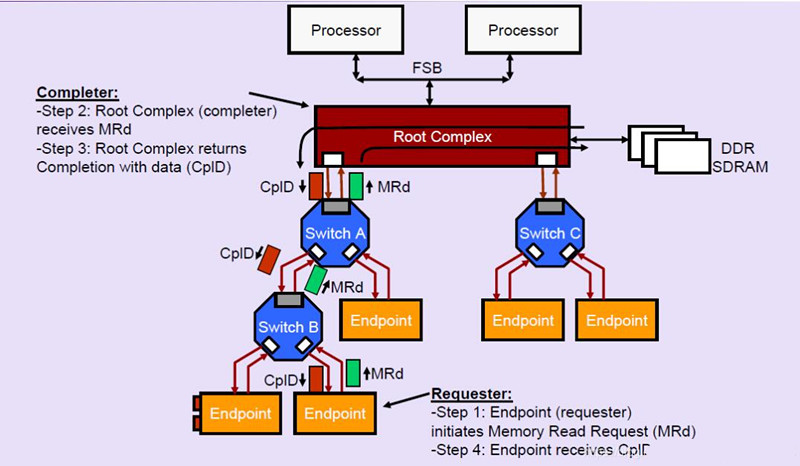
3、Transfer between end point and end piont
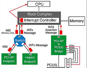
Interrupt types of PCIE
There are two main types of interrupts for PCIE.
1、MSI:Message interrupt
2、INTx:Pin interrupt
True PCIe devices: must use MSI to send interrupts, can optionally support INTx messages.
PCI devices: must support INTx messages
Theoretical bandwidth of PCIE
Gen2 unidirectional link rate 5Gbps
1、 Use 8B/10B encoding, incurring 20% data overhead
2, Theoretical bandwidth = link rate 80% number of channels
3、 For single channel.
- Gen1: 2.5Gbps0.8=250MBps
- Gen2: 5Gbps0.8=500MBps
- Gen3: 8Gbps*1=1GBps
- More overhead is caused by the protocol
- Data Header
- Checksum bits
- Link training
- Error communication
Brief description of TLP packet format
We have already explained the common types of TLP packets above, so this part explains the specific format of each TLP packet.
The format of a TLP packet is as follows.
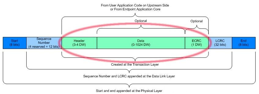
The details of each are as follows.
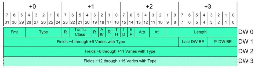
Next, a rough introduction to each of the above.
1、Fmt :It is used to indicate whether the TLP package is 3DW or 4DW
2, Type: used to determine the type of TLP packet
Memory read or write
CompleTIon packet
ConfiguraTIon packet
Message
3, Traffic Class: In addition to MemoryRead/Write TLPs must be zero, the general case is the default is 0
4, Attr : contains specific information about the core behavior when processing transactions
5, TD: When the bit is 1, the TLP package includes CRC checks, when zero does not include CRC checks
6, EP: indicates that this TLP contains errors and should be ignored
7, AT: Address type, generally default to zero can be.
Default/Untranslated (00)
TranslaTIon Request (10)
Translated (11)
8、Length Field :Describe the length of the valid data of the TLP packet, note that the unit DW, the maximum length of 1024 DW length
9, First/Last Byte Enables: Each of the four bits corresponds to the validity of each byte in the first DW and the last DW of the TLP packet. A DW is exactly 4 bytes as well.
Memory Write TLP Header Format
The Memory Write TLP Header format is as follows.
TLP packet header for 3DW.
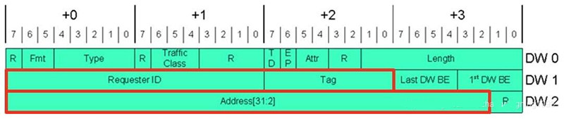
4DW’s TLP package head.

1、Requester ID: including bus, device, and funcTIon numbers these in the ID routing when the necessary information
2, Tag: defined by the user, the specific content and role of the user to negotiate.
3、Address: byte address, the lowest two are always zero-aligned to the DWord addressing.
Memory Read TLP Header format
Memory Read TLP Header format is as follows.
3DW TLP packet header.

4DW’s TLP package head.

1, Tag – Here the Tag is mainly used to return to the CplDs package reorganization, because the meal back to the completion of the package is not necessarily in order to return.
There is no new bit introduced here, we have finished introducing it in the previous.
Memory Read is Non-Posted.
Non-Posted requests always generate a completion packet in response. Posted requests never generate a completion packet unless there is an error. A typical MRd generates a completion with a packet. A Read request can generate one or more completion packets.
Completions TLPs Format

1, Tag: Here you need to pay attention to the Tag flag is mainly for the receiving end in accordance with the order of packets sent
2、Lower Address: indicates the lower bit of the byte address of the first enabled data byte, the lower address and length cannot span an RCB
RCB: Read Completion Boundary
3, Byte count: indicates the number of bytes remaining before the request is satisfied
4、Completion status: Just the status of the completion packet.
Successful completion (“000”)
Unsupported request (“001”)
Configuration request retry status (“010”)
Completer abort (“100”)
5、Requester ID : ID of the device requesting CplD (bus, device, function)
6、Completer ID : ID of the device that is building CplD (bus, device, function)
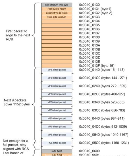
The return must be an integer multiple of RCB. And the first one should be aligned with the RCB, and can not exceed MPS, here is an official example given.
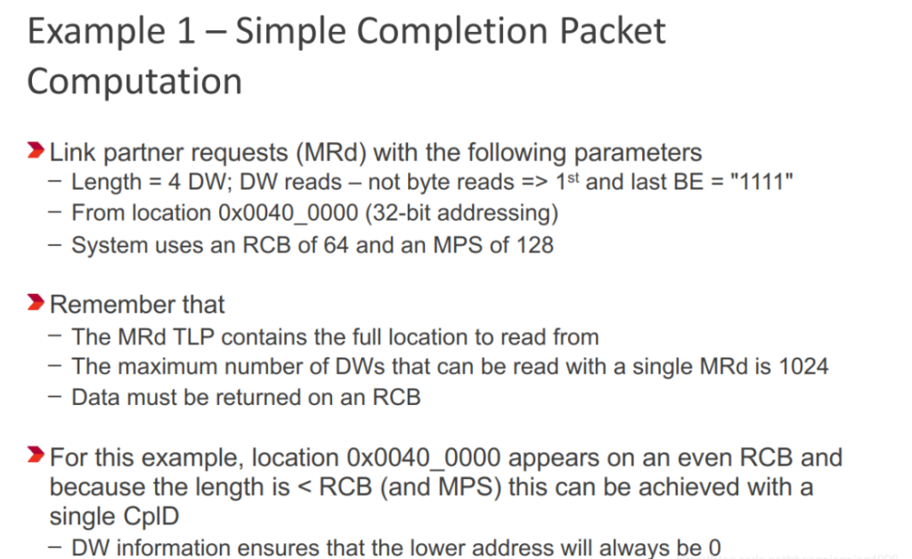
Example 2.
Title.
Solution.


Message/Message with Data TLP format

Since we generally do not use it for manual group information packets, we will not go into detail here.
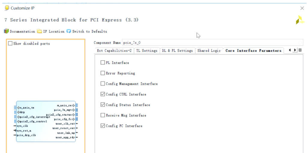
PCIE IP core configuration needs attention
Here is a brief introduction to the PCIE core configuration process, this time we do not use XDMA IP, use the following PCIE IP:
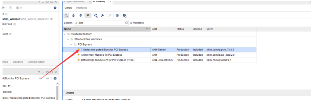
To learn as much as possible about the details in PCIE IP, we have selected Advanced IP Customization:.

1, select advanced IP customization, for users to choose more features
2, here you can choose whether this PCIE IP core is used as endpoint or root port
3, this is to specify the PCIE IP and then the hardware location number
4, specify the number of PCIE lanes
5、Specify the maximum communication speed of a lanes
6, the PCIE will be converted to AXI4 protocol clock
7、Convert PCIE to AXI4 protocol data bit width
8、Reference frequency of PCIE IP

1、Vendor ID, the ID of the PCIE that belongs exclusively to Xilinx, is fixed.
2、Device ID, together with the vendor ID, specifies the type of data that is used to select the software driver of the PCIE upper unit.
3, Version ID, specifying the version to be set using this PCIE IP
4, Sub-vendor ID, used to more closely distinguish the Xilinx vendors
5、Subsystem ID, used to identify the ID of the board
The above values can generally be default, do not need to do much processing
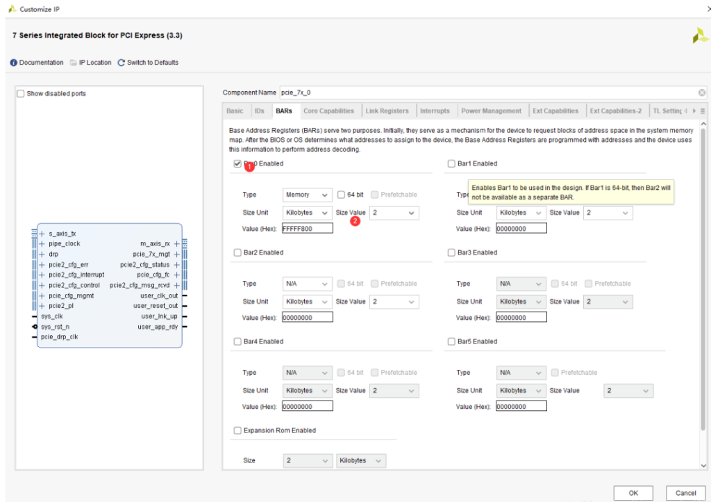
- Select Enable Bar Space. It should be noted here that the root port’s access to the endpoint can only access the bar space, while the endpoint’s read and write operations to the root port can access the entire memory.
- Select whether the address of the Bar is 32-bit or 64-bit. The space size is generally selected as 1K, which is only used to transfer some commands. The size of its value is related to the size of the space, the specific relationship is not clear here.
The entire setting above, and then the PCIE header configuration space are reflected in.

1, here you can add buffer for optimization, the rest of the default can be.
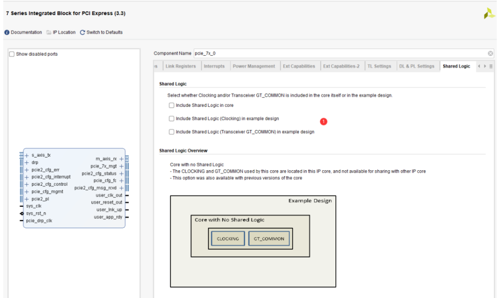
1, here we generally do not choose to share logic

1, pin interrupt, the traditional sense of interrupt, in PCIE is basically no longer used
2、Message interrupt, more commonly used in PCIE