Are you an electronics designer looking to reduce PCB space and cost?
Does your design require high levels of intelligent processing and compute performance per watt?
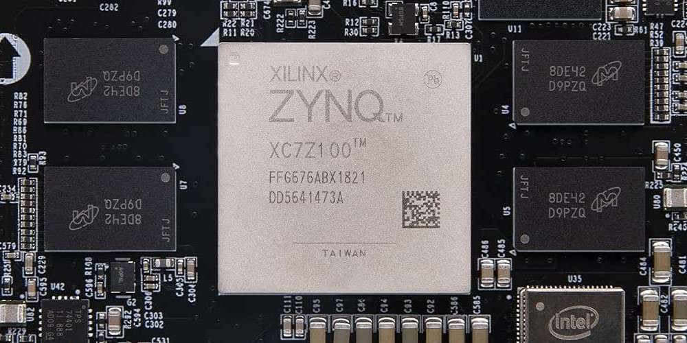
You have probably been working on various types of FPGA architecture, but you may not have tried the Xilinx Zynq 7000 soc and FPGA. Of course, no other company comes close to integrating CPU and FPGA in a single die. According to Raff Schaffer, project lead at Agilent Life Science Group, it was only made possible by Xilinx with the Xilinx zynq 7000 soc.
This article caught your attention if you have read to this point. Please find interesting facts about the Xilinx Zynq 7000 soc and why you should start building with it. This article will explain the following about Xilinx Zynq 7000 soc;
- What is the Xilinx Zynq 7000?
- Why should you build with the Xilinx Zynq 7000 soc?
- What is the difference between a Zynq Chip and an FPGA?
- What type of operating system does the Zynq operate?
WHAT IS THE XILINX ZYNQ 7000 SOC?
The Xilinx Zynq 7000 soc is the first in the industry to support the software programmability of a processor. It is also the first generation of an extensible processing platform (EPP).
Its performance per watt and scalability show that the Zynq 7000 soc programmable logic supports quick parallel processing of extensive data. It combines flexibility, scalability, and performance, thus bringing SoC design to a whole new level. Another edge it has is the ability to;
- Support systems require high-end marketing applications and multifunctionality. In addition, it provides a basis for mixed-signal functionality with its core arm cortex A9.
- Zynq 7000 supports real-time system responsiveness beyond what is obtainable in conventional processing system solutions by technology.
- Zynq 7000 provides an IP ecosystem on multiple levels using the vivado design suite.
- It aids software acceleration and wired, wireless communications. In addition, the hardware development resources are second to none.
KEY DIFFERENCE BETWEEN ZYNQ CHIP AND AN FPGA
As a designer, one would undoubtedly have had some basic historical knowledge of FPGAs, ASICs, or ASSPs. However, for this article, it is necessary to know why Xilinx developed the Zynq 7000 soc.
- ASICs AND ASSPs
As with ASSPs and ASICs, these processors come with a defined level of performance. It was challenging to add flexibility to allow for other operations. The need for SoCs arose with design kit complexity. - FPGAs
FPGAs were deemed better than ASICs and ASSPs, but FPGAs consumed more power and less performance. Moreover, the FPGAs could not match the fully integrated SoCs, which led to Xilinx building the Zynq 7000 soc. - ZYNQ CHIPS
In straightforward terms, the difference between Zynq 7000 soc and FPGAs is the provision of a dual-core processor that supports optimized architecture architected with just a single device.- It also supports the use of customized accelerators and peripherals for embedded development.
- Unlike FPGAs, Zynq 7000 guarantees low latency, maximum design flexibility, and adaptive computing.
- Unlike FPGAs, there is a faster time to market with maximum reuse without jeopardizing performance.
- Zynq 7000 cortex A9 uses a single chip with AI inference acceleration on the embedded applications.
5 REASONS WHY SHOULD YOU BUILD WITH THE ZYNQ 7000 SOC
REASON 1: Most Efficient FPGA and ARM For Analytics And Control
- Each Zynq 7000 soc comes with a 1GHz dual-core ARM Cortex A9 microprocessor. The two processors communicate with the SDRAM and flash memory controllers, on-chip-memory, and the extended blocks. This communication is possible through the ARM-AXI-based interconnect. It also provides a better environment for a complete embedded processing platform.
- The programmable system-on-chip processor system (PS) is attached to the programmable logic (PL) of the Zynq device. This connection is made via the ARM-AXI ports to provide more efficient coupling and performance.
- Depending on your preferred bandwidth selection on the Zqnq PS, you can select the number and size of ARM AXI PS-PL connections. The PS has four 64/32-bits configurable high-performance AXI ports, which supply the programmable logic with direct high-speed access to the Zynq 7000 soc.
REASON 2: Industry-Leading High-Level Synthesis
- The secret of going from algorithm to high-speed logic within the shortest period is known as high-level synthesis (HLS). Zynq 7000 allow algorithm developers to write their codes in C, C++, or system C. After registering, it also allows you to debug it on PCs and servers.
However, once the algorithm becomes successful, you can simply recompile the code to run on one of the Zynq 7000 platforms ARM Cortex-A9 MPCore processors. Isn’t this beautiful?
So what if the implementation is not as fast as you want it? Not too worry!
You may consider physical implementation using logic cells to recode high-level algorithms written in those languages. However, this process is usually slow until the introduction of HLS. Designers now feed their algorithm into the HLS tool, then receive the code needed to implement hardware acceleration.
REASON 3: Highest Level Of Reliability And Security
- The Zynq 7000 soc cortex A9 supports intelligent systems’ high reliability and tight security. One important safety measure is that the Zynq 7000 allows processor booting first before the xilinx FPGA side. The booting system also supports sequence user authentication (RSA), data authentication (HMA), and encryption (AES-256).
- Xilinx also includes an anti-tamper technology (AT) necessary for both defense systems on modules (SOMs) and commercial users.
Apart from the operational reliability of system parameters, the Xilinx SoCs design supports the 28nm testing method. This testing method eliminates memory errors, especially in aerospace defense and consumer electronics.
REASON 4: MOST CONTROL EXTENSIVE OS, STACK ECOSYSTEM, AND MIDDLEWARE
- Conventionally, every hardware requires software to operate efficiently. Therefore, Xilinx designed the Zynq 7000 cortex A9 with embedded vision and maximum flexibility with the following features.
- Support Linux variant OS (PetaLinux by Xilinx, Wind River’s Linux 5, and Timesys’ LinuxLink).
- Support the Android from idea and Adeneo, Microsoft’s Windows Embedded Compact 7.
- Various real-time operating systems such as;
- Xilinx’s FreeRTOS
- Express Logic’s ThreadX/NetX.
- Green Hills Software’s INTEGRITY.
- Mentor Embedded’s Nucleus.
- ETAS’ RTA-OS SC1-4.
- Also, Xilinx Zynq 7000 cortex A9 provides an unmatched software IP ecosystem on multiple levels with software development systems such as;
- Green Hills Software
- Kyoto Microcomputer
- ARM
- Abatron
- Computex
- Microsoft
- Yokogawa.
- Znyc 7000 also supports a wide range of middleware and stack vendors explicitly designed for ARM Cortex-A9 MPCore. It also enhances the IP ecosystem on multiple levels. These processors include the following;
- Secure system operation.
- Image processing and recognition.
- Face recognition
- Imaging
- Graphics
- Video codecs
- Audio codecs
- File systems
- Databases
- Networking
REASON 5: LOWEST SYSTEM POWER AND FASTEST LOGIC FABRIC
- The Xilinx SoCs allow customers to choose the 28nm programmable logic of either the Xilinx kintex 7 or Artix 7. The kintex 7 is best for a low-cost development board and high performance with all the essential components. Conversely, the Artix 7 is best for the lowest power and cost while delivering twice the performance of the spartan 6.
It also supports a scalable platform of the optimized architecture of kintex seven and Artix 7 fabrics. Depending on operation requirements, the Artix 7 can offer an average of 15% higher performance. The Kintex 7 can also provide a standard of 50% faster 28nm performance of unique application requirements.
DESIGN FLOW OF THE ZYNQ 7000 SOC ARCHITECTURE
If you are already familiar with the design flow of FPGAs and development tools, this is similar to what you know. The stages are as follows;
- Define the specifications and requirements of the system.
- Next is task partitioning (assigning functions in either PL or PS): How a designer defines this task can significantly affect the overall system performance. Therefore, they should administer great care during the hardware or software implementation.
- The next stage is testing the hardware and software development tools: The designer should know what to expect during the testing.
- Testing Programmable Logic
The designer should identify the functional blocks needed to achieve the desired characteristics. Also, the blocks will assemble as IPs while making necessary connections.
- Testing Processing System
Ensure that there is software security integration delivering code on the PS. Thus, system integration and testing are needed to wrap up the design.
- Testing Programmable Logic
- Application Processing Unit (APU)
This unit contains two ARM cortex a9 processing systems with both carrying a NEON unit, floating-point unit (FPU), memory management unit (MMU), and L1 cache. Also, the APU contains a snoop control unit (SCU) with L2 caches. Below is a brief explanation of what each of these units does;- MMU: The MMU translates the virtual memory addresses to the physical memory addresses.
- Snoop Control Unit (SCU): The L1 and L2 caches are an interface task among the dual-core processors.
- L2 cache: It is between the two processors that enable them to access the newest update of a variable.
- NEON: This unit provides the Single Instruction Multiple Data (SIMD) which brings significant acceleration of DSP and media algorithms to the central ARM processor.
- FPU: This unit provides the acceleration for the floating-point operations.
CONCLUSION
The Zynq 7000 SOC, with all the essential components and the Cortex A9, has come to revolutionize devices. Xilinx also made the process of its processing system and hardware programmability easy with the Vivado design suite.