The Xilinx ZCU102 is an Evaluation board that features Zynq Ultrascale + TM MPSOC with a dual-core Cortex-R5F real-time processor and quad-core Arm Cortex-A53. This board combines a processing system and user-programmable logic in the same device.
Also, ZCU102 offers support for major interfaces and peripherals. Therefore, this board is ideal for use in high-performance applications. Xilinx ZCU102 offers great features and benefits.
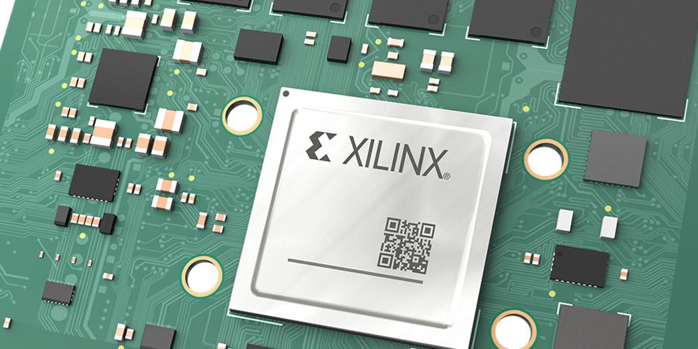
What is Xilinx ZCU102?
Xilinx ZCU102 allows designers to make designs for industrial, communications, and automotive applications. It is an Evaluation board that features Zynq Ultrascale + TM MPSOC with a dual-core Cortex-R5F real-time processor and quad-core Arm Cortex-A53. This board combines a processing system and user-programmable logic in the same device Also, ZCU102 offers support to major interfaces and peripherals. Therefore, this ensures development for various applications.
Xilinx ZCU102 comes with -2 speed grade devices. Also, the support for multiple speed grades demands adjustments of voltage. The programmable logic VCCINT supply will be adjustable through PMBUS. There are three processing units in the Zynq Ultrascale + TM MPSOC. These processing units include:
- Mali-400 graphics processing unit with pixel and geometry processor.
- Cortex-R5 real-time processing unit-Arm V8 architecture
- Cortex-A53 APU-Arm V8 architecture-based 64-bit quad-core multiprocessing CPU
Zynq Ultrascale + TM MPSOC features four main high-speed serial I/O (HSSIO) interfaces that supports these protocols:
- SATA 3.1 specification interface
- USB 3.0 specification integrating a 5 GB/s line rate
The PL and PS can couple with several signals and interfaces to implement user-created hardware accelerators. Also, they integrate other functions in the PL that are very accessible to the processors. Also, they can access memory resources in the PS.
The PS I/O shares a multiplexed I/O of about 78 multiplexed I/O pins. Also, Zynq Ultrascale + TM MPSOC utilize I/O in the PL domain for several PS I/O peripherals. You can achieve this through an extended MIO and boots at reset or power-up.
USB 2.0 ULPI PHY and USB 3.0 Transceiver
Xilinx ZCU102 utilizes a standard USB 2.0 ULPI transceiver and USB3320 to support a link to the host computer. There is a USB cable in the ZCU102 evaluation kit. Also, the USB3320 supports the UTMI + low pin interface standard. The ULPI standard has defined the interface between the PHY device and USB controller IP. This drives the physical USB bus.
He ULPI standard minimizes the number of interface pins between the PHY device and the USB controller IP. A 24 MHz crystal will clock the USB3320. Through the IP in the PS of XCU9EG MPSOC, you can implement the interface to the USB3320 PHY.
Furthermore, you can tie the USB 3.0 micro B connector shield to GND by using a jumper on a header. Therefore, the USB shield can connect via a capacitor to GND by the installation of a capacitor. The USB3320 ULPI U116 transceiver circuit features a MIC2544 high-side programmable current limit switch. This switch features an open dria fault flag on pin 2. If there are thermal shutdowns or overcurrent shutdown conditions, the fault flag will turn on LED DS51. DS51 is in the U116 circuit area close to the push-button SW2.
Clock Generation
Xilinx ZCU102 offers variable and fixed clock sources for XCU9EG MPSOC.
Programmable user clock
Xilinx ZCU102 comprises a differential oscillator linked to the GC inputs of PL bank. The output frequency within 10 MHz and 810 MHz can change user applications. Also, you can power cycle the ZCU102 board to revert the user clock to a default frequency. Furthermore, you can reprogram the oscillator from the MSp430 system controller.
Programmable User MGT Clock
Xilinx ZCU102 features a programmable low-jitter differential oscillator linked to a 1-to-2 clock driver. The user clock will default to an output frequency once you power up. Also, user applications can alter the output frequency within 10MHz and 810 MHz via a 12C interface. Power cycling Xilinx ZCU102 will revert the user clock to a default frequency. You can reprogram the oscillator from the MSP430 system controller.
User SMA MGT Clock

Xilinx ZCU102 includes a pair of SMAs for a differential AC. Also, the differential signal pair is coupled as a series-capacitor.
CP1208 USB UART Interface
The CP2108 quad on the Xilinx ZCU102 board offers four level-shifted UART links via a single micro-B USB connector. Channel 1 and 0 are PS-side MIO connections. Also, Channel 3 and Channel 2 is typically connected to MSP430 system controller U41.
CP2108 channel 2 Pl-side
This channel 2 interface circuit offers connections from XCZU9EG MPSoC U1.
CP2108 channel 3
The CP2108 channel 3 channel UART interface circuit links from MSP430 U41 to CP2108 u40.
HDMI Clock Recovery
Xilinx ZCU102 board features Silicon Labs. The Si5324 jitter generates the reference clock for the transmitter subsystem when you use the HDMI transmitter as a standalone. Also, the Si5324 functions in free mode and utilizes an external oscillator. The Si5324 produces a jitter-annuated reference clock. Also, the HDMI IP controls the jitter enable functions and S15324 clock.
ZCU102 comprises a small form-factor pluggable quad-connector that accepts SFP + modules. The main purpose of the SFP/SFP+ clock is to offer support to synchronous protocols like OBSAI or CPRI to carry out clock recovery. Also, the S15328B configuration occurs in free-run mode. Therefore, this allows the jitter attenuation feature.
Electrostatic Discharge Caution
Electrostatic discharge (ESD) can destroy electronic components when they are not properly handled. Therefore, this can lead to intermittent or total failures. Also, it is important you follow some prevention procedures when handling components. Therefore, to prevent ESD damage, follow these instructions:
- Ensure you use the ankle strap or ESD wrist. Then connect the end of the strap of the equipment to a metal surface on the chassis.
- The wrist strap shields components from ESD on only the body. Therefore, don’t touch the adapter against your clothing.
- Don’t touch the printed circuit board
- Ensure you place the adapter on an antistatic surface
Conclusion
Xilinx ZCU102 comprises great features which make it an outstanding evaluation board. One of the great benefits of this board is that it supports major interfaces and peripherals. We have discussed the major elements of this evaluation board in this article.