Introduction
XDMA (Xilinx Direct Memory Access) is a high-performance direct memory access engine developed by Xilinx for use in their FPGA and ACAP products. XDMA provides an efficient means of transferring data between FPGA logic and processing system memory while offloading the Central Processing Unit (CPU).
Key features of XDMA include:
- Direct transfers between FPGA and memory without CPU involvement
- Scatter-gather DMA capability
- Multiple DMA channels
- Configurable transfer burst size
- Interfaces such as PCI Express, memory-mapped AXI
- Optimized for local or remote transfers
- Reference design available from Xilinx
XDMA delivers flexible, high-speed DMA capability to maximize data throughput for memory-intensive FPGA applications.
XDMA Architecture
The XDMA architecture consists of control and data transfer paths to manage DMA transfers independently of the system CPU.
Control Path
The control path coordinates and manages the DMA channels and transactions. Key components include:
- DMA engine – processes transfer requests and handles transfers
- Register space – configures DMA channels and options
- Interrupt controller – generates interrupts to signal events
- Scatter-gather engine – chained descriptor transfers
The control logic automates DMA transfers so the CPU is not burdened.
Data Path
The data path provides the direct transfer of data between FPGA logic and memory:
- Read/write engines – source and sink data
- Data FIFOs – buffer data during transfers
- Bus interfaces – AXI, PCIe, etc. for system connection
Bulk data flows directly via the data path without needing to go through the CPU.
XDMA Transfer Modes
XDMA supports several DMA transfer modes to provide flexibility:
- Simple DMA – single contiguous block transfer
- Scatter-gather DMA – multiple concatenated block transfers
- Interrupt coalescing – consolidate interrupt signals
- Automatic SG chaining – link scatter-gather blocks
- Multichannel DMA – independent concurrent transfers
- Generic sideband signals – custom handshaking
The transfer modes can be combined and tailored to optimize different DMA workflows.
XDMA Software Drivers
To control XDMA from a CPU, Xilinx provides software drivers for either Linux or standalone environments:
- Linux driver – control XDMA as a Linux kernel driver
- Standalone driver – manage XDMA bare-metal without OS
- Common software interface – consistent API for both environments
- Userspace tools – application utilities for testing
- Reference design test benches – simulation test cases
The drivers and tools speed up the development of software to manage DMA transfers.
XDMA Benefits
Using XDMA for FPGA data transfers provides several advantages:
- Accelerates throughput for memory-intensive applications
- Reduces CPU overhead by offloading data copying
- Optimizes system performance through asynchronous operation
- Better determinism with fixed transfers
- Simplifies data streaming architectures
- Leverages native bus protocols like PCI Express, AXI
- Reference design available for fast integration
For data-driven systems, XDMA delivers high efficiency gains.
XDMA Application Examples
XDMA has widespread use for applications such as:
High Performance Computing
- Efficient clustering using FPGA acceleration cards
- Low latency data transfers between processing nodes
- Burst transfers to move large data sets
Data Acquisition
- High-speed sensor acquisition to memory
- Buffering and emptying image capture buffers
- Low overhead for transferring large samples
Networking
- Packet processing offload
- Rapid spooling of data to processors
- Low jitter quality of service traffic handling
Embedded Systems
- Coprocessing sensor fusion and analytics
- Offloading data preprocessing from microcontrollers
- Real-time data capture and control loops
XDMA enables building high-speed interfaces, hardware offload engines, and more to maximize system performance.
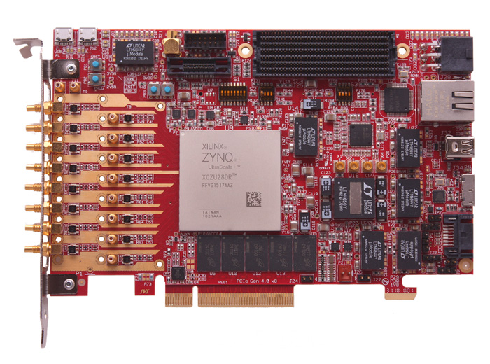
XDMA Integrated Block for PCIe Designs
For FPGA designs using PCI Express, Xilinx provides an integrated XDMA block that optimizes PCIe DMA transfers.
Key features of the integrated XDMA block:
- Configurable number of channels (1 to 16)
- 128-256 bit AXI stream interfaces
- SG descriptor fetch/update in HW
- Multiple completion notification options
- Configurable product ID, vendor ID
- Optimized for Ultrascale PCIe interface
The integrated block allows rapid deployment of an optimized PCIe XDMA solution.
Conclusion
Xilinx XDMA provides an efficient direct memory access capability for Xilinx FPGA and ACAP designs. By offloading data transfers from the CPU, XDMA maximizes throughput for memory and I/O intensive applications. The flexible transfer modes and software drivers enable tailoring XDMA to specialized use cases and rapid integration with hardware designs. For data-focused acceleration and offload, XDMA is an enabling productivity-boosting technology.
XDMA FAQ
Here are some common questions about Xilinx XDMA:
What are the typical data transfer rates supported by XDMA?
XDMA transfer speeds depend on the interface, but often exceed multiple GB/s for interfaces like PCIe Gen3 x8. Near line rate throughput is possible.
What Xilinx FPGA families support XDMA?
The major families with XDMA support include Zynq UltraScale+, Virtex UltraScale+, Kintex UltraScale, and Versal ACAPs. Older families have alternative DMA.
What are the typical steps to integrate XDMA into an FPGA design?
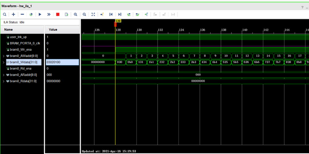
Typical integration involves instantiating the XDMA IP core, connecting AXI stream interfaces, connecting interrupts, and parameterizing options like number of channels. The provided reference design is a good starting point.
What processors work with XDMA?
The Linux kernel driver supports ARM and PowerPC processors for XDMA control. The standalone driver can work with any processor supporting memory-mapped access like MicroBlaze.
What tools are needed to develop with XDMA?
Vivado IP integrator can configure the XDMA core. Software development uses standard tools like compilers, debuggers, the Xilinx SDK, and utilities like DMA test scripts.
The Evolution of Xilinx XDMA and Xilinx Converged Memory Access
RDMA and Xilinx converged memory access are two methods of RDMA communication. They both have advantages and disadvantages. This article will explore the evolution of these technologies and what they can offer to developers. It also looks at RDMA over Ethernet and PCIe. This technology allows developers to use memory-mapped FPGA components and resources. However, it is not a substitute for other methods of RDMA communication.
RDMA
Xilinx’s RDMA evolution IP core is an innovative, parameterizable solution for converging ethernet and wireless applications. It provides high throughput, low latency, and hardware offload reliability of data transfer. It can simultaneously connect to many remote hosts with a single physical interface and includes a Linux driver for easy integration into embedded systems. In addition, it is compatible with ARM processors.
RDMA is a popular technology in the detector community. In addition, its ability to support a wide variety of communication protocols has attracted the attention of researchers in the field of high-performance X-ray crystallography.
Xilinx XDMA
Xilinx PCIe solutions offer a broad range of options and flexibility for designing high-performance, low-power applications. These products include PCIe bridge hard and soft IP blocks, memory-mapped FPGA components, and reference designs. In addition, Xilinx PCIe solutions include Integrated Blocks (IBs) that enable high-performance InfiniBand connectivity and support for remote direct accelerator memory access.
InfiniBand is one implementation of RDMA. Today, consolidated implementations of RDMA support ethernet, iWARP, and OmniPath. These platforms provide native support for Linux and Windows and add additional support for other systems. In addition, Xilinx XDMA is available for many popular processors and platforms, including ARM, RISC-V, and AVR.
RDMA over Ethernet
RDMA over Ethernet (RDMAoE) is an industry-standard for interconnecting FPGAs and Ethernet switches. It is compatible with Xilinx UltraScale+ FPGAs and Mellanox adapters. However, there are some drawbacks. The RDMA protocol is not yet as widely supported as InfiniBand.
RDMA over ethernet is a highly reliable, high-throughput data transfer interface. It allows applications to access remote node memory with a single chip. In addition, InfiniBand provides support for remote direct memory access. This allows the host CPU to focus on other tasks while leaving RDMA to the network adapter. It also eliminates memory copy operations between user application memory and the operating system data buffer, reducing the transfer latencies and increasing throughput.
RDMA over PCIe
Xilinx RDMA over PCIe is an advanced DMA solution for the PCIe standard. We can implement it on many Xilinx devices, including the Xilinx 7 series ARM processors, Xilinx XT devices, and UltraScale devices. In addition, it is an open-source solution that uses the DMA ranges property of the PCIe host controller to initiate transfers.
Xilinx RDMA over PCIe enables a faster data transfer speed by using a single chip for multiple purposes. It is also available in a reference design that provides the underlying hardware design files for the DMA implementation. This reference design contains both VHDL and Verilog HDL simulation models. In addition, the DMA library provides a DDR-RAM interface driver that allows data to be transferred directly to and from memory without the processor’s involvement. Finally, Xilinx RDMA over PCIe is also available as an open-source reference design.
RDMA over InfiniBand
Xilinx’s RDMA over InfiniBand IP can be helpful in various applications. RDMA is a single-sided communication protocol that allows data to pass from one device to another. RDMA uses an Ethernet interface to achieve this. Although RDMA had initial support on InfiniBand, consolidated implementations of RDMA are available for ethernet, such as RDMA over Converged Ethernet (RoCE). The Xilinx XDMA IP is also compatible with several other systems, including Windows and Linux.
RDMA over InfiniBand is a common networking technology, but it can also be helpful in applications that don’t require fail-safe communication. However, RDMA is not ideal for fail-safe applications such as Class III medical devices, nuclear facilities, airbag deployment applications, and life-support systems. Therefore, Xilinx recommends that designers not use RDMA in critical applications.
Using Xilinx XDMA in Your Project
The Xilinx XDMA is an excellent tool for PCIe bridges, but it is limited in what it can do. As the name implies, it is limited to one PCIe channel and cannot add anymore. Furthermore, it is invisible to the user and, thus, not suitable for advanced DMA implementation. If you want to use Xilinx XDMA in your project, here are some useful tips.
Xilinx xdma blocks
Xilinx enables PCIe bridge and DMA implementation with its Xilinx DS-DMA subsystem. Both devices offer PCIe and DDR4 interfaces. The Xilinx DS-DMA blocks and Xilinx IP Integrator (IPI) can be helpful together for PCIe and DDR4 support. As with other Xilinx DS-DMA blocks, a developer should be able to design a simple DMA test component using just a few lines of code.
Xilinx xdma driver
The Xilinx mxFPGA XDMA driver is the application that generates and manages device files. It transfers data from the FPGA to the CPU or vice-versa. The device files should end in either h2c_0 or c2h_0. You can create them with /dev/xdma0/ or /dev/xdma0_, respectively.
The Xilinx FPGA XDMA driver for PCIe and DDR4 is a component of the mxFPGA software. In addition, the xdma driver is part of the mxFPGA software, which we can download from the Xilinx website. As a result, the xdma driver can be helpful in various applications.
Xilinx xdma architecture
Xilinx’s XDMA architecture has been around for several years. As a result, the design is very easy and straightforward. Its architecture consists of the AXI to Native block and the Native to PCIe bridge. The AXI to Native block defines the register interface signals that communicate with the PCIe interface. The Native signal, on the other hand, interacts with the outside world through the PCIe interface.
PCIe is a common protocol for high-speed data transmission. This architecture is compatible with various CPUs, including the Xilinx PCIe core. In addition, the POWERPC-compatible VxWorks software provides the Xilinx PCIe driver with easy register access. The Xilinx XC7k325T FPGA can use this driver to read and write DDR3 memory and measure the speed through PCIe.
Xilinx xdma size
To ensure that your Xilinx PCIe DMA Subsystem will perform optimally, you’ll want to know the best way to set it up and use it. For optimal performance, use software to test different options. Among these are the optimal transfer size and polling. The following are some tips for optimizing performance with Xilinx PCIe DMA Subsystem.
Interrupt processing
The Xilinx XDMA chip supports PCIe interconnect and includes an initial driver and an IRQ-based addressing scheme for a PCIe bridge. However, its limitations make it unsuitable for advanced DMA implementation. The XDMA wrapper supports PCIe link rates Gen1 (2.5 GT/s) and Gen2 (5.0 GT/s).
A chip can use a programmable register during interrupt processing to handle XDMA messages. The IRQ_DUMP() function returns a list of transfer variables, ep_addr, and -ENOMEM. This routine then waits for the w_timeout, which is a fixed period. A PCI-compatible register struct may use one of these methods, but a recursive call can be a better solution.
In addition, the Xilinx IRQ-V and XdMa IO interface allow interrupt handling and masking. A good example is to create a user-mode interrupt handler. If you’re unfamiliar with interrupt handling, you can learn Rayming PCB & Assembly basics. Then, when you’ve mastered WinDriver, you can begin programming your ARM device with Xilinx XDMA interconnect.
If you’re designing a RISC-V-based ARM processor, you should be aware that the interrupt processing method can significantly affect the data throughput. The DMA writes an interrupt to the host, then waits for an ISR to process it. This process can take time, and you shouldn’t rely on this method. MSI-X interrupts, on the other hand, offer better data rates.