Xilinx is well-known for designing high performance CPLD. The Complex Programmable Logic Device (CPLD) by Xilinx is a combination of a bank of macrocells and a fully programmable array. Macrocells refer to functional blocks that carry out sequential or combinational logic. Also, these cells feature added flexibility.
CPLDs have always used analog sense amplifiers for enhancing their architectures’ performance. Also, CPLDs execute various functions in systems design as a result of their capabilities. Xilinx understands the benefits of using CPLDs. Therefore, it has been able to design the Xilinx XC9572XL. In this article we will be focusing on Xilinx XC9572XL High Performance CPLD.
What is Xilinx XC9572XL?
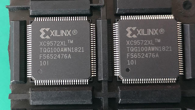
Xilinx XC9572XL is a CPLD specifically designed for low-voltage and high-performance applications in communications and computing systems. Also, it comprises four 54V18 Function Blocks that offer 1,600 usable gates. Xilinx FPGA XC9572XL offers a lot of advanced system features and high I/O per macrocell counts.
Also, this device can fit easily into existing design flow. Therefore, this helps to save time and simplify design. With the Xilinx XC9572XL, it is impossible to steal stored designs. This device features improved security. Also, it is reprogrammable to fix any system bugs.
Xilinx XC9572XL features 5 ns pin-to-pin logic delays. Also, the system frequency of this device is about 178 MHz. The Xilinx XC9572XL architecture offers 72 macrocells with 1,600 usable gates. This device is optimized for high level performance 3.3V systems. Therefore, it offers low power operation and Fast FLASHTM technology.
Xilinx XC9572XL fully supports IEEE standard 1149.1 boundary-scan (JTAG). This allows great debug and design iteration for small footprint packages. Also, this device provides a low-power operation for each macrocells. Therefore, this enables device power to be significantly minimized. The user may program each macrocell in low-power mode.
The Xilinx XC9572XL family is specially developed to work with Spartan-XL and Xilinx Virtex. Therefore, this enables system designers to separate logic optimally between high-density general purpose logic and fast interface circuitry. Also, the XC9572XL family is pin-compatible. This makes design migration across several density options in a particular package footprint easy.
There are several function blocks and I/O blocks in the XC9572XL device. This device is a subsystem. The I/O block offers buffering for device outputs and inputs. Every functional block (FB) offers programmable logic capability. Also, the FastCONNECT II switch matrix links all input signals and FB outputs to the FB inputs.
Features of Xilinx XC9572XL
Xilinx XC9572XL comprises several features. These features are responsible for the performance of this complex programmable logic device.
Fast concurrent programming
Xilinx XC9572XL is highly preferred among other CPLD devices due to its fast concurrent programming. Also, it is widely used by competitive programmers due to its programming speed. In addition, this device supports in-system programming (ISP).
Excellent reliability and endurance
Xilinx XC9572XL features excellent quality. Also, it is very reliable. This device offers at least an endurance level of 10,000 in-system programs or erase cycles. Also, it provides data retention for at least 20 years. Every device meets all data retention specifications and functional performance within the endurance limit
Improved design security
Xilinx XC9572XL CPLD integrates enhanced data security features. Therefore, this prevents the programming data from any inadvertent device reprogramming or erasure. Also, the user can set the read security bits to prevent reading the internal programming pattern. After setting these bits, they can possess further program operations.
There are write security bits in this device. Therefore, this offers extra protection against any accidental device reprogramming when JTAG pins are exposed to noise.
5V tolerant I/Os
The I/Os on every Xilinx XC9572XL device are completely 5V tolerant although the core power supply is 3.3 volts. Therefore, this enables 5V CMOS signals to directly connect to the XC9572XL inputs without any damage. Also, you can apply the 3.3V Vccint power supply after or before applying 5V signals to the I/Os. The Xilinx XC9572XL devices have protection against power supply sequencing problems.
Optimized for high performance 3.3V systems
This device is optimized for high performance 3.3V systems. Therefore, it includes low power operation. Also, its 5V tolerant I/O pins can accept 2.5V, 5V, and 3.3V signals. Xilinx XC9572XL CPLD features Fast FlashTM technology. This technology offers high performance logic capability and superior reliability. Also, this technology provides endurance ratings and fast programming times.
Small footprint packages
You can have Xilinx XC9572XL devices in small footprint packages. These packages include 44-pin PLCC, 48-pin CSP, 100-pin TQFP, 44-pin VQFP, and 64-pin VQFP. Also, there is PB-free for all packages.
Advanced System Features of Xilinx XC9572XL High Performance CPLD
Xilinx XC9572XL includes some advanced system features which makes it a high performance CPLD. Below are some advanced system features of this device:
- It features In-system programmability
- It has full IEEE standard 1149.1 boundary-scan (JTAG)
- Also, there is a local clock inversion with one product-term clocks and three global clocks.
- All user pin inputs comprises a bus-hold circuitry
- Also, it comes with advanced pin-locking and routability
- It features about 90 product-terms for each macrocell with allocation of individual product-term
- Also, it has very wide 54-input function blocks
- It comprises individual output enable for each output pin
- Also, it features input hysteresis on all boundary-scan and user pin inputs
Power Estimation in Xilinx XC9572XL CPLD
In CPLDs, power dissipation can vary substantially based on the system frequency and output loading. Also, design applications can determine power dissipation. You can configure every macrocell in Xilinx XC9572XL CPLD for low-power mode. This helps to minimize power dissipation. Also, the software automatically deactivates macrocells and unused product terms. Therefore, this helps to conserve power.
You can use the following equation for an estimate of Icc.
ICC(mA) = MCHS(0.175*PTHS + 0.345) + MCLP(0.052*PTLP + 0.272) + 0.04 * MCTOG(MCHS +MC)
Here
- MCHS refers to the macrocells in high-speed configuration
- MCLP is the #macrocells in low power configuration
- f refers to the maximum clock frequency
- PTLP refers to the average number of low power product terms for each macrocell
- PTHS refers to the average number of high-speed product terms for each macrocell
- MCTOG refers to the average % of flip-flops per clock
The Architectural Description of XC9572XL
There are several units that make up the Xilinx XC9572XL.
Function block (FB)
Every function block comprises independent macrocells. Also, the function block receives output enable, reset/set, and global clock signals. This block produces outputs that help the FastCONNECT switch matrix. A sum-of-products representation helps to implement the logic within the FB.
Macrocell
Every macrocell in XC9572XL can be separately configured for a registered or combinatorial function. You can configure the macrocell register as a T-type or D-Type flip-flop. Also, you can bypass it for combinatorial operation. Every register provides support for asynchronous reset and set operations.
FastCONNECT II switch matrix
This connects signals to the function block inputs. All I/O block outputs and all functional block outputs drive this matrix.
Input/output block
The I/O Block, also known as IOB interfaces between the device user I/O pins and internal logic. Every IOB comprises an output enable selection multiplexer and output driver. Also, each IOB features user programmable ground control and an input buffer.
Every IOB offers user programmable ground pin capability. Therefore, this enables you to configure device I/O pins as additional ground pins. This will force unused pins to a low voltage condition. Each I/O block offers bus-hold circuitry that remains active when there is valid user operation. Also, the bus-hold property removes the need to tie unused pins low or high.
You can configure every output driver for slew-rate limited operation. Every output driver can offer fast switching with reduced power noise. All output drivers may have grounding capability. You can achieve this by internal logic. The IOB is a crucial element in the Xilinx XC9572XL series FPGA.
Xilinx XC9572XL Devices
The Xilinx XC9572XL series FPGA features several devices. Some of these devices are below.
XC9572XL-10CS48I XC9572XL-10TQG100C XC9572XL-10TQ100C
XC9572XL-5TQG100C XC9572XL-10VQG64I XC9572XL-7VQG64I
XC9572XL-5VQ44C0962 XC9572XL-5CSG48C XC9572XL10VQ44C0962
XC9572XL-7VQ64I0962 XC9572XL-10TQ100C4766 XC9572XL-7VQ64C0962
XC9572XL-10VQ44C0818 XC9572XL-10VQG44C XC9572XL-10VQG64C
XC9572XL-7CSG48C XC9572XL-5TQ100C0962 XC9572XL-5VQ64C0962
XC9572XL-10VQ44I4766 XC9572XL-10VQ44Q0100 XC9572XL-10VQ44I0962
Features of XC9572XL-10CS48I
XC9572XL-10CS48I is a high performance complex programmable logic device that comprises the following features:
- It has Pb-free for all packages
- Has enhanced 0.35 micron feature size CMOS
- Also, it features a local clock inversion with one product-term and three global clocks
- Supports Full IEEE standard 1149.1 boundary-scan JTAG
- Come with Improved data security
- Its endurance exceeds 10,000 erase/program cycles
- It has pin-compatible with 5V-core XC9572 device in the 100-pin TQFP package
- Comprises input hysteresis on all boundary-scan and user pin inputs
- Also, it comes with 5V tolerant I/O pins that accept 3.3V, 5V, and 2.V signals
- Its system frequency is about 178MHz
- Also, it has 2.5V or 3.3V output capability
- It is in-system programmable
- Furthermore, it comprises pin-locking and routability with Fast CONNECTTM II switch matrix
- It has 20 year data retention
- Also, its ESD protection exceeds 2,000V
- Comes with wide 54-input function blocks
Features of XC9572XL-10TQG100C
- It has pin-compatible with 5V-core XC9572 device in the 100-pin TQFP package
- Comprises input hysteresis on all boundary-scan and user pin inputs
- Also, it comes with 5V tolerant I/O pins that accept 3.3V, 5V, and 2.V signals
- Its system frequency is about 178MHz
- Also, it has 2.5V or 3.3V output capability
- It is in-system programmable
- Furthermore, it comprises pin-locking and routability with Fast CONNECTTM II switch matrix
- It has 20 year data retention
- Also, its ESD protection exceeds 2,000V
- Comes with wide 54-input function blocks
- It has Pb-free for all packages
- Has enhanced 0.35 micron feature size CMOS
- Also, it features a local clock inversion with one product-term and three global clocks
- Supports Full IEEE standard 1149.1 boundary-scan JTAG
- Come with Improved data security
- Its endurance exceeds 10,000 erase/program cycles
Features of XC9572XL-10TQ100C
- Supports Full IEEE standard 1149.1 boundary-scan JTAG
- Come with Improved data security
- Its endurance exceeds 10,000 erase/program cycles
- Comes with wide 54-input function blocks
- It has Pb-free for all packages
- Has enhanced 0.35 micron feature size CMOS
- Furthermore, it comprises pin-locking and routability with Fast CONNECTTM II switch matrix
- Also, its ESD protection exceeds 2,000V
- Has 20 year data retention
- It has pin-compatible with 5V-core XC9572 device in the 100-pin TQFP package
- Comprises input hysteresis on all boundary-scan and user pin inputs
- Also, it comes with 5V tolerant I/O pins that accept 3.3V, 5V, and 2.V signals
- Its system frequency is about 178MHz
- Also, it has 2.5V or 3.3V output capability
- It is in-system programmable
Features of XC9572XL-5TQG100C
- It has Pb-free for all packages
- Has enhanced 0.35 micron feature size CMOS
- Also, it features a local clock inversion with one product-term and three global clocks
- Supports Full IEEE standard 1149.1 boundary-scan JTAG
- Come with Improved data security
- Its endurance exceeds 10,000 erase/program cycles
- It has pin-compatible with 5V-core XC9572 device in the 100-pin TQFP package
- Comprises input hysteresis on all boundary-scan and user pin inputs
- Also, it comes with 5V tolerant I/O pins that accept 3.3V, 5V, and 2.V signals
- Its system frequency is about 178MHz
- Also, it has 2.5V or 3.3V output capability
- It is in-system programmable
- Furthermore, it comprises pin-locking and routability with Fast CONNECTTM II switch matrix
- It has 20 year data retention
- Also, its ESD protection exceeds 2,000V
- Comes with wide 54-input function blocks
Features of XC9572XL-10VQG64I
- It has pin-compatible with 5V-core XC9572 device in the 100-pin TQFP package
- Comprises input hysteresis on all boundary-scan and user pin inputs
- Also, it comes with 5V tolerant I/O pins that accept 3.3V, 5V, and 2.V signals
- Its system frequency is about 178MHz
- Also, it has 2.5V or 3.3V output capability
- It is in-system programmable
- Furthermore, it comprises pin-locking and routability with Fast CONNECTTM II switch matrix
- It has 20 year data retention
- Also, its ESD protection exceeds 2,000V
- Comes with wide 54-input function blocks
- It has Pb-free for all packages
- Has enhanced 0.35 micron feature size CMOS
- Also, it features a local clock inversion with one product-term and three global clocks
- Supports Full IEEE standard 1149.1 boundary-scan JTAG
- Come with Improved data security
- Its endurance exceeds 10,000 erase/program cycles
Conclusion
CPLDs are ideal for use in several applications. The XC9572XL CPLD by Xilinx has proved to be useful in low-voltage and high performance applications. It is widely used in computing and communication systems. This article has reviewed the features of Xilinx XC9572XL devices.