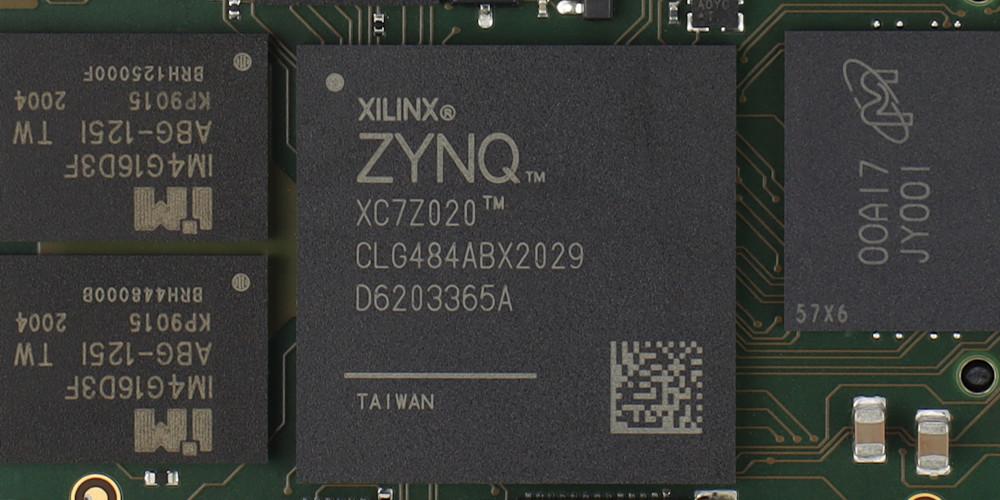
The Xilinx XC7Z020 is a FPGA that offers ideal scalability and flexibility. This FPGA offers vast benefits when used in extremely critical applications. in this article, we will focus more on how the XC7Z020 series works in applications.
What is the Xilinx XC7Z020?
The XC7Z020 series is based in the SoC architecture by Xilinx. The devices here incorporate a single-core or dual-core ARM. The XC7Z020 FPGA Core Board comprises all basic components of hardware. This board supports embedded processing. It comprises 28 nm Xilinx programmable logic (PL) and cortexTM-A9 based processing system (PS) in a single device. Also, the ARM Cortes-A9 CPUs comprises external memory interfaces, on-chip memory, and peripheral connectivity interfaces.
Xilinx XC7Z020 provides the scalability and flexibility of a field programmable gate array. Also, this series offer ease of use and great performance associated with ASSPs and ASIC. The XC7Z020 family comprises devices that enable designers to focus on cost-sensitive applications from a platform. The Xilinx FPGA XC7Z020 can be useful in a wide range of applications like broadcast camera, multifunction printers, and industrial motor control.
Also, it is widely used in applications like medical diagnostics and imaging, machine vision, and baseband among others. The architecture of Xilinx XC7Z020 allows users to integrate custom software in the PS and custom logic in the PL. Also, the integration of the PL and PS enables performance levels two chip solutions can’t match. This is because of their limited power budgets and I/O bandwidth.
Xilinx provides several soft IP for the XC7Z020 family. For peripherals in the PL and the PS, there are Linux device drivers and stand-alone. Also, the implementation of the ARM-based PS offers a wide range of third-party tools. The application processor allows high-level OS support e.g, Linux. Also, the PL and PS are on different power domains which enable the user to manage the power of the PL.
The Processor System of Xilinx XC7Z020
There are four major blocks in the PS. These blocks are:
- Interconnect
- Memory interfaces
- Application processor unit (APU)
- I/O peripherals (IOP)
Interconnect
Interconnect provides support for several simultaneous master-slave transactions. Also, it is specifically designed with ARM CPU and bandwidth critical masters like the PL masters. Multilayered ARM AMBA AXI interconnect connects the IOP, APU, and memory interface to each other. The Quality of Service (QoS) block can regulate traffic through the interconnect. Also, the QoS feature helps to control traffic produced by the CPU, DMA controller.
Memory interfaces
This unit comprises a static memory interface and a dynamic memory controller. Also, the static memory controller supports a parallel NOR flash interface and a parallel data bus. You can configure the multi-protocol DDR memory controller to offer 16-bit or 32-bit wide accesses. The dynamic memory controller supports LPDDR2, DDR3, DDR2, and DDR3L. Also, the DDR memory controller allows the PL and PS to have a shared access to a common memory. The static memory interfaces offer support to external static memories.
Application processor unit (APU)
The APU comprises the following key features:
- Operates in symmetric dual processor, asymmetric dual processor mode, and single processor
- NEON media processing engine
- Double and single precision floating point
- Integrated memory management unit (MMU)
- ACP Accelerator coherency port interface that enables coherent accesses from PL to CPU memory space
- CoreSight debug and trace support for Cortex-A9
I/O peripherals
This unit comprises the data communication peripherals. The main features of the I/O peripherals consist of :
- Two USB 2.0 OTG peripherals, each of these support about 12 endpoints
- Two UARTs
- About 118 GPIO bits
- Two full CAN 2.0B compliant CAN bus interface controllers
- Two full-duplex SPI ports having three peripheral chip selects
The I/O peripherals relate to external devices via a shared pool of about 54 dedicated multiuse I/O pins. Also, every peripheral can have one of pre-defined groups of pins. This allows a flexible assignment of several devices simultaneously. Also, the majority of IOP interface signals are available to the PL. Therefore, this enables the use of standard programmable logic I/O pins when configured properly. All multiuse I/O pins offer support to 1.8V HSTL.
The Programmable Logic (PL)
The PL comprises main features like:
- Programmable I/O blocks
- 36 kb block Ram
- DSP slices
- PL configuration module
- Low-power serial transceivers in selected device
- PL configuration module
Digital Signal Processing –DSP Slice
The DSP applications make use of several binary accumulators and multipliers. These are best integrated in dedicated DSP slices. Every DSP slice comprises a 48-bit accumulator and a dedicated 25 X 18 bit two’s complement multiplier. Also, the multiplier and accumulator can both operate about 741 MHz.
Also, the DSP comprises an additional pre-adder, used in symmetrical filters. Also, this pre-adder enhances performance in packed designs. In addition, it can minimize DSP slice count by almost 50%. DSP also consists of a 48-bit-wide Pattern Detector used for convergent rounding. Also, the pattern detector can integrate 96-bit-wide logic functions when utilized with a logic unit.
Also, the DSP slice offers extension capabilities and extensive pipelining that boost the efficiency and speed of several applications more than digital signal processing. The accumulator can also serve as a synchronous up/down counter.
Block RAM
Block RAM comprises major features like:
Synchronous operation
The clock controls every memory access. Also, it registers all clock enables, write enables, address, and inputs. Also, the input address is usually clocked. Therefore, it retains data until the next operation. There is an optional output pipeline register that enables high clock rates at the expense of additional cycle of latency. Also, the data output can reveal the newly written data or previously stored one during a write operation.
Error detection and correction
Every 64-bit-wide block RAM can produce and use extra Hamming code bits. With this, it can perform double-bit detection of error and single-bit error correction during the read process.
Programmable data width
You can configure every port as 16K x 2, 1K x 36, and more. There can be different aspect ratios for the two ports without constraints. Every block RAM can be in completely independent 18Kb block RAMs.
FIFO controller
There is a built-in FIFO controller for dual-clock or single-clock operation which increments the internal addresses. Also, it offers four handshaking flags like almost empty, almost full, empty, and full. You can freely program the almost empty and almost full flags.
Input/Output
The programmable I/O functionality features:
- High-frequency decoupling capacitors for improved signal integrity
- Digitally controlled impedance that can be high speed I/O operation
- High-performance SelectIOTM technology
The device and package size determines the number of I/O pins. Every I/O can comply with a big number of I/o standards. All other programmable pins feature similar I/O capabilities. The SelectIO resources in Xilinx XC7Z020 are either high performance (HP) or high range (HR). The HR I/Os provide the broadest range of voltage support. Also, the HP I/Os are for the highest performance operation ranging from 1.3V to 1.8V.
The Xilinx XC7Z020 utilizes various package types to meet the needs of the user. This includes small form factor wire-bond packages.
Low-power serial transceivers
The low-power serial transceivers feature the following:
- Decision feedback equalization (DFE) and adaptive equalization for more margin
- High-performance GTX transceivers that have about 12.5 Gb/s line rates
- Low-power mode for chip-to-chip interfaces
The transceiver counts are from 0-16 transceiver circuits. Also, every serial transceiver is a receiver and transmitter. The different serial transceivers can combine LC tank architecture and ring oscillators to enable a blend of performance and flexibility.
- Receiver
This is a serial-to-parallel converter. It transforms the incoming bit-serial differential signal into parallel words. Therefore, the designer can easily trade-off internal datapath. Also, the receiver gets the incoming differential data stream and then feeds it via programmable linear.
- Transmitter
This is a parallel-to-serial converter. Also, it has a conversion ratio of 20, 32, 80, 64, 40, and 16. Therefore, the designer can trade-off width for timing margin.
Applications of Xilinx XC7Z020 Series
The Xilinx XC7Z020 is widely used in several applications like:
- Night vision and video equipment
- Broadcast camera
- IP and smart camera
- Multifunction printers
- Machine vision, industrial motor control, and industrial networking
- Baseband and LTE radio
- Medical diagnostics and imaging
- Automotive driver assistance
Some Devices in Xilinx XC7Z020 Series
XC7Z020-2CLG484I XC7Z020-2CLG400I XC7Z020-DIE0628
XC7Z020-ICLG40014410 XC7Z020-ICLG400C4759 XC7Z020-2CL40014480
Features of XC7Z020-2CLG400I
- It has ARM Cortex™-A9
- Has PS Terminal 1GB DDR3, 32bit
- Comes with 32MB FLASH
- Comprises several Logic Cells
- Also, it has 53,200 Look-Up Tables (LUTs)
- CLB Flip-Flops 106,400
- It comprises 220 DSP Slices
- Its working temperature ranges from -40oC to 85oC
Features of XC7Z020-2CLG484I
- It has embedded Dual-Core ARM Cortex-A9 Processor
- Comes with 1GByte DDR3, 32bit, 1066Mbps
- Also, it comprises 32MByte QSPI Flash, 8GByte EMMC
- It has HDMI Output Interface and supports 1080@60Hz, 3D Output
- Also, it offers documents in PDF (Schematic, PCB, Chip Datasheet and User Manual)
- It offers Verilog HDL demos and supporting Tutorials
- It comprises One Gigabit Ethernet on the PS Side and four Gigabit Ethernet Ports on the PL Side
- There is 40-pin expansion port for module
- It comes with USB Uart, Integrated USB, SD Card Slot, and other interfaces
Conclusion
Xilinx XC7Z020 series offer ease of use and great performance associated with ASSPs and ASIC. Also, this series comprises devices that enable designers to focus on cost-sensitive applications from a platform. The Xilinx XC7Z020 can be useful in a wide range of applications like broadcast camera, multifunction printers, and more.