Introduction
The Xilinx XC6SLX100-2FGG676I is a high-end FPGA (Field Programmable Gate Array) in the Spartan-6 family. With an abundance of logic cells, ample memory, and high-speed transceivers, this device provides a powerful foundation for advanced programmable logic designs.
Some key features of the XC6SLX100 FPGA include:
- Built on low-power 45nm process
- Contains 147,443 logic cells
- 12.9 Mb block RAM capacity
- 700 DSP48A1 slices with 25×18 multipliers
- Multi-gigabit serial transceivers
- 1020 programmable I/O pins
- Advanced power management options
- High-density 676-pin BGA package
In this overview, we will explore the XC6SLX100 architecture, functionality, design tools, and applications to better appreciate the capabilities of this FPGA.
XC6SLX100 Architecture
The XC6SLX100 utilizes a streamlined architecture to provide abundant programmable logic.
Configurable Logic Blocks
The core of the FPGA consists of slices containing:
- 4 LUTs and 8 flip-flops per slice
- Specialized carry logic circuits
- Distributed memory in LUTs
The XC6SLX100 contains a total of 147,443 slices, organized into 11,661 CLBs.
Block RAM
12.9Mb of dual-port block RAM provides on-chip data storage:
- 300 blocks of 36Kb each
- True dual read/write ports
- Configurable as RAM, ROM or FIFO
Block RAM enables buffering data without consuming logic resources.
DSP Slices
700 dedicated low-power DSP slices provide:
- 25 x 18 bit signed multipliers
- 48-bit adder/accumulators
- Hardware cascade connections
DSP slices are optimized for digital signal processing functions.
I/O
The FPGA includes:
- 1020 user I/O pins
- Support for common I/O standards
- High-speed serial transceivers
Abundant flexible I/O enables interconnection to a wide range of components.
XC6SLX100 Features
Key features and specs of the Xilinx XC6SLX100-2FGG676I FPGA include:
Logic Cells
- 147,443 logic slices
- 589,772 LUTs
- 1.18 million flip-flops
Block RAM
- 12.9Mb total RAM
- 300 x 36Kb blocks
DSP Slices
- 700 x DSP48A1 slices
Transceivers
- 12 x 3.6Gbps RocketIO
I/O Pins
- 1020 user I/O
- Flexible I/O standards
Power
- 45nm low-power process
- 1.0V core voltage
- 15-20W total power
Packaging
- 35mm x 35mm, 1.0mm pitch
- 676-pin fine-pitch BGA
XC6SLX100 Design Tools
Xilinx provides the ISE Design Suite for developing with Spartan-6 FPGAs:
ISE WebPACK
- VHDL and Verilog HDL design entry
- XST synthesizer for logic synthesis
- Map, place and route to FPGA
- ISim simulator
ChipScope Pro
- Analyze and debug logic post-synthesis
- Virtual I/O, logic analyzer
EDK Embedded Tools
- Build Microblaze embedded processors
- Create peripherals, stacks, drivers
- Debug deployed systems
Robust tools maximize productivity for Spartan-6 FPGA development.
XC6SLX100 Applications
The combination of programmable logic, DSP, and transceivers enables the XC6SLX100 to excel in:
- Wireless and wireline communications
- Image, video, and signal processing
- Test and measurement systems
- Industrial automation and motor control
- Aerospace and scientific computing
- Prototyping and pre-silicon validation
For these embedded digital systems, the XC6SLX100 provides outstanding performance per watt.
Comparison to Kintex-7 FPGA
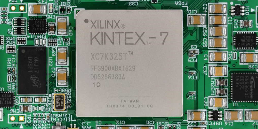
Compared to the newer high-end Kintex-7 FPGA:
- Kintex-7 utilizes smaller 28nm process vs 45nm
- Kintex-7 provides over 2x the logic capacity
- Kintex-7 transceivers reach up to 28Gbps vs 3.6Gbps
- Kintex-7 has higher performance PCIe Gen3 interfacing
- Kintex-7 adds 100G Ethernet MAC blocks
- Kintex-7 has advanced power management techniques
Kintex-7 represents a major boost in capability over Spartan-6 generation.
Conclusion
The Xilinx XC6SLX100 packs high-end Spartan-6 programmable logic capability into a space-saving 35mm x 35mm package. With abundant logic cells, ample dual-port block RAM, dedicated DSP slices, multi-gigabit transceivers, and feature-rich I/O, the XC6SLX100 tackles demanding applications. The ISE Design Suite provides proven tools to maximize design productivity. Offering FPGA-class capabilities at CPLD cost levels, the XC6SLX100 provides outstanding value for complex digital systems.
XC6SLX100 FPGA FAQ
Here are some common questions about the Xilinx XC6SLX100 FPGA:
What design entry methods can be used for the XC6SLX100?
VHDL, Verilog, and schematic capture are supported. These synthesize into the FPGA fabric using XST.
What are the typical clock rates supported in the XC6SLX100?
The FPGA logic can operate up to 500MHz+ speeds. The I/O transceivers support up to 3.6Gbps.
What core supply voltage does the XC6SLX100 require?
The FPGA core logic operates at 1.0V nominal voltage. Periphery I/O supports 1.2-3.3V signaling standards.
How much block RAM is available in the XC6SLX100?
It contains 300 x 36Kb blocks providing a total of 12.9Mb RAM, configurable as smaller memories.
How does the XC6SLX100 compare to the lower cost XC6SLX25T?
The XC6SLX100 offers much higher logic capacity, transceivers, DSP slices and block RAM vs the more compact XC6SLX25T.