Introduction
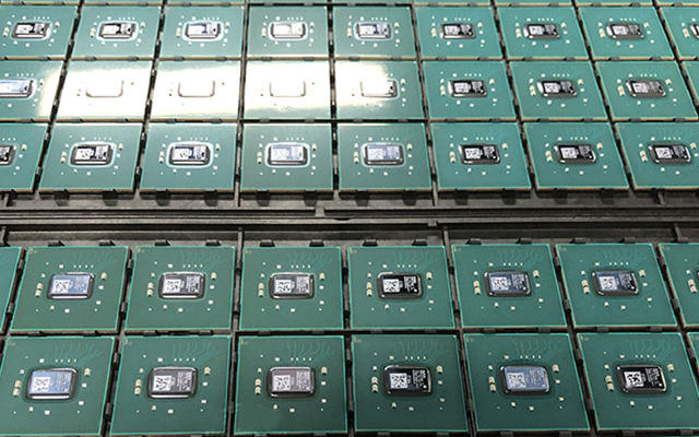
The Xilinx xc2c64a-7vqg100c is a mid-range FPGA (Field Programmable Gate Array) belonging to the CoolRunner-II CPLD family. Released in 2005, this device provides 64 macrocells of in-system programmable logic along with abundant functionality and I/O in a space-saving form factor.
Some key features of the xc2c64a-7vqg100c:
- In-system programmable logic
- 64 macrocells with product term sharing
- 1.8V VCCINT nominal core power supply
- High density VQ100 package
- PLL, DLL, DCM clock management
- 5V tolerant selectable I/O standards
- Low static and dynamic power consumption
In this article, we dive into the xc2c64a architecture, capabilities, design tools, and applications to better understand this flexible CPLD.
xc2c64a Architecture
The xc2c64a contains multiple functional elements interconnected to provide flexible logic and I/O.
Logic Array Blocks
The core programmable logic consists of 4 Logic Array Blocks (LABs). Each LAB provides:
- 16 macrocells for logic implementation
- Product term sharing for efficiency
- Local interconnect arrangement
With 4 LABs, the xc2c64a contains 64 macrocells of logic.
Input/Output Blocks
Integrated I/O blocks provide:
- 66 user I/O pins
- 5V tolerant selectable standards
- Multi-voltage support 1.5V/2.5V/3.3V
- Adjustable drive strength and slew
- Digitally controlled impedance
- On-chip termination
Flexible I/O enables interfacing to common standards.
Clock Management
Two digital clock managers (DCMs) and a phase-locked loop (PLL) provide:
- Delay locked loops for I/O timing alignment
- Zero delay buffers, frequency synthesis
- Phase shifting, clock deskew
- Low jitter clock generation
Advanced clock management allows timing closure even at high clock rates.
This combination of programmable logic, abundant I/O, and clocking resources makes the xc2c64a a capable CPLD.
xc2c64a Features
Here are some of the key features and specs of the xc2c64a FPGA:
Programmable Logic
- 64 macrocells in 4 Logic Array Blocks
- 288 product terms shared across macrocells
- 2 or 4 inputs per macrocell
- Local LAB interconnect
Clocking
- 2 Digital Clock Managers
- Phase Locked Loop
- Zero delay buffers
I/O
- Up to 66 user I/O pins
- Multi-voltage support 1.5/2.5/3.3V
- 5V tolerant selectable standards
- 1.8Gbps data rates
Static Power
- 1.8V VCCINT supply
- 15mA typical ICCINT quiescent
Packages
- FineLine BGA footprint
- 17mm x 17mm, 0.8mm ball pitch
- 100-ball VQ100 package
- Commercial and industrial grades
xc2c64a Design Tools
Xilinx provides robust design tools for the CoolRunner-II family:
ISE Design Suite
- VHDL and Verilog support
- XST synthesis tool
- Floorplanner for constraint-driven layout
- Timing analyzer
- Waveform viewer
- Smart compile and smart guide
CoolRunner-II CPLD Designer
- Windows graphical design capture
- Drag and drop macrocell logic building
- Automatic resource allocation
- Timing driven placement and routing
- Multi-language simulation
Alliance Software
- Low cost design entry
- VHDL and Verilog support
- Simulation and verification
A complete tool suite supports the full development cycle.
xc2c64a Applications
With its balance of capacity, performance, and cost-efficiency the xc2c64a suits many applications:
- Automotive – body controllers, engine control
- Industrial – motor drives, instrumentation
- Consumer – printers, scanners, cameras
- Communications – gateways, network cards
- General logic integration and glue logic
The xc2c64a hits a sweet spot between basic CPLDs and higher cost FPGAs.
xc2c64a vs. CoolRunner XPLA3
The xc2c64a provides higher performance than the preceding XPLA3 generation:
Logic Cells
- 64 macrocells vs 32 macrocells for XPLA3
- More product terms and inputs per macrocell
Clocking
- DCM for clock synthesis and alignment
- PLL for low jitter generation
I/O
- 1.8Gbps data rate vs 660Mbps
- Lower pin-to-pin delays
Power
- 1.8V core vs 3.3V supply for XPLA3
- 70% lower ICCINT quiescent
Cost
- Higher density at lower cost per macrocell
The xc2c64a boosted CPLD capability to the next level over XPLA3.
Conclusion
The Xilinx xc2c64a-7vqg100c provides a versatile blend of medium-density logic, abundant high-speed I/O, and advanced clock management. Built on a proven architecture, the xc2c64a delivers an optimized balance of capability, power efficiency, and cost. With over a decade of use across industries, this CoolRunner-II CPLD continues serving as a workhorse for a wide range of applications.
xc2c64a FPGA FAQ
Here are some common questions about the xc2c64a CPLD:
What design tools can program the xc2c64a FPGA?
The Xilinx ISE Design Suite provides the primary development tools. This includes design entry, synthesis, place and route, and configuration.
What voltage does the xc2c64a core operate at?
It uses a 1.8V VCCINT nominal power supply for the internal FPGA core logic. Periphery I/O supports 1.5V, 2.5V, and 3.3V standards.
What package options are available for the xc2c64a?
The main package is the 17mm x 17mm 100-pin VQ100 BGA. Other options include TQ100 and PQ100 packages with -6 speed grades.
How much static power does the xc2c64a consume?
Typical ICCINT quiescent current is 15mA. Maximum ICCINT static current is 100mA.
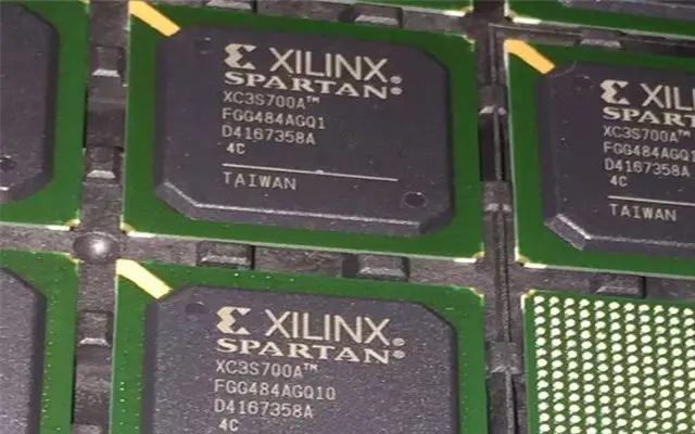
What are some key differences between the xc2c64a and the Spartan-3 series?
The Spartan-3 is an FPGA with much higher capacity, performance and logic-oriented features. The xc2c64a is a CPLD focused more on simple glue logic and I/O integration.
XC2C64A-7VQG100C belongs to the XC2C64A Field Programmable Gate Array (FPGA) series by Xilinx. It is a CoolRunner-powered circuit with 64-macrocells that are optimally designed for use in both low and high-performance applications.
FPGA consumers typically go for this when looking for circuit devices that improve both the system reliance and performance.
The XC2C64A-7VQG100C is used in a wide range of industries, including but not limited to:
- Medical equipment
- Artificial Intelligence
- The Internet of Things (IoT)
- Consumer electronics
- 5G technology
- Industrial control
- Cloud computing
- Wireless technology
Technical Specifications of the XC2C64A-7VQG100C:
Below is a tabular representation of the technical attributes of the XC2C64A-7VQG100C FPGA:
| Technical Attributes | Descriptions |
| Mounting Style | Surface Mount Technology (SMT) |
| Number of Input & Output (I/O) Pins | 64 |
| Supply Voltage (DC) | 1.80 V |
| Lead-Free Status | Lead-Free |
| Package/Case | 100-TQFP |
| RoHS Status | Compliant |
| Lifecycle Status | Active |
Features of XC2C64A-7VQG100C
These are some of the distinctive features that make XC2C64A-7VQG100C better than the other Field Programmable Gate Arrays (FPGAs) out there:
1. Combinational Modes of Operation
XC2C64A-7VQG100C has eight (8) Function Blocks that are interconnected to operate via a low-power AIM – Advanced Interconnect Matrix. The AIM works by supplying up to 40 complementing inputs to the Function Blocks.
Already, the Function Blocks have 16 Macrocells and a 40 x 56 P-term PLA. The combinational modes of XC2C64A-7VQG100C’s operation are derived from the several configuration bits that have been configured into the board.
2. Dual Performance Applications
There is no need to get separate circuits for low-power applications and high-power applications. The dual performance of the XC2C64A-7VQG100C already provides for that.
On the lower power aspect, the circuit relies on its dynamic operation and stand-by power to improve the overall performance of the system.
The high-powered application bolsters the speed of the battery-operated devices. It also helps in saving power, especially for high-end communication equipment.
3. RealDigital Design Technology
One of the reasons why the performance of battery-powered devices manufactured with XC2C64A-7VQG100C offers better performance and power-saving is because of the RealDigital Design Technology.
By default, the technology combines with the CMOS technology to improve the fabrication and design of the board. This also goes a long way to improve the performance of the circuit board, as well as reduce the power consumption on the board.
4. 1.8 V Optimization
Field Programmable Gate Arrays (FPGAs) are now being optimized for use on circuits with a temperature range up to 1.8 V. This is the reason for optimizing the XC2C64A-7VQG100C for 1.8 V systems.
The advantages of this include but are not limited to the reduction of the quiescent current and improved performance via the 4.6 ns pin-to-pin logic delays.
5. Clocking Availability
Clocks are readily available on the XC2C64A-7VQG100C. For emphasis, the clocks in the microcell registers can be configured individually. That way, the performance can be improved up to zero.
On the other hand, clock synchronization is attained via the three (3) global clocks enabled in the Function Blocks.
Wrapping Up
RayPCB can help configure your XC2C64A-7VQG100C to fit into high-performance and low-power applications. We can also model the Integrated Circuit (IC) to work on devices across multi-industry facets, such as A.I., IoT, and consumer electronics.