Introduction
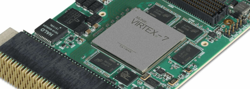
The Xilinx Virtex-7 FPGA is a high-performance programmable logic device that provides advanced capabilities for the most demanding electronic systems designs. As part of the high-end Virtex family, the Virtex-7 offers an ideal mix of capabilities to implement DSP, embedded processors, high-speed serial connectivity, logic density, and advanced packaging.
In this comprehensive guide, we will explore the architecture, features, applications, and design tools of the Virtex-7 to understand why it is a popular choice for today’s complex FPGA-based designs.
Virtex-7 Family Overview
The Xilinx Virtex-7 family consists of five major product families to address different application requirements:
- Virtex-7 FPGA
- Virtex-7 H580T FPGA
- Virtex-7 HT FPGA
- Virtex-7 2000T FPGA
- Virtex-7 XT FPGA
The Virtex-7 FPGAs are the most versatile and highest volume family, while the others provide optimizations for cost, power efficiency, maximum density, and extreme performance.
Within each family, there are multiple device/package combinations to choose from depending on I/O pin count, transceiver lanes, memory, DSP blocks and other resources required. Supported package types range from flip-chip BGA packages to large, high-pin count PQFP packages.
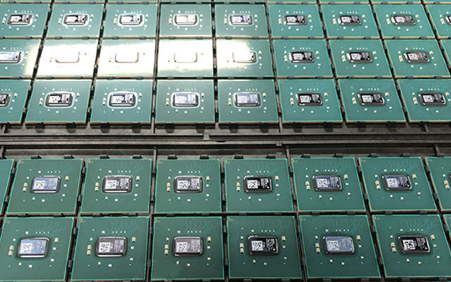
All Virtex-7 families are fabricated on a high-performance 28nm manufacturing process. They provide 1.9V core voltage and offer SECDED and dynamic bit error detection for reliability.
Virtex-7 FPGA Architecture
The core Virtex-7 FPGA architecture provides a balanced set of resources well-suited for a wide range of applications:
- Configurable Logic Blocks (CLB) – The basic logic building block, each CLB includes LUTs and flip-flops for implementing synchronous logic. Virtex-7 provides up to 792,00 CLBs.
- DSP Slices – Dedicated arithmetic resources optimized for DSP and math intensive algorithms. Provide 25×18 signed multipliers. Virtex-7 has up to 2016 DSP slices.
- Block RAM (BRAM) – On-chip data storage, each BRAM block is 36 Kbits. Virtex-7 has up to 6.8 Mb of total BRAM.
- Transceivers – High-speed serial interfaces up to 28 Gbps. Virtex-7 provides up to 48 transceivers depending on the device.
- Mixed-Mode Clock Manager (MMCM) – Flexible clock synthesis, timing and jitter control. Virtex-7 includes up to 13 MMCMs.
- PCI Express Blocks – Integrated Gen3 x8 PCIe hard blocks for high-performance interconnect.
- Configurable I/O – Flexible, high-performance I/O supporting common standards like DDR3, PCIe, DisplayPort, GigE etc.
- Processor System – Hard microprocessor system based on dual ARM Cortex-A9 MPCore with peripherals.
This balanced architecture enables creating systems with the right mix of programmable logic, memory, DSP resources, connectivity, and processors in a single device.
Virtex-7 FPGA Features
Let’s take a closer look at some of the major features of the Virtex-7 architecture:
CLBs – Configurable Logic Blocks
The CLB is the basic building block of logic in the Virtex-7. Each CLB includes:
- 2 slices, each with 4 LUTs and 8 flip-flops
- Cascade circuitry between slices
- Fast carry logic
- Wide multiplexers
LUTs are fundamental programmable elements used to implement logic functions. Virtex-7 CLB provides advanced 6-input LUTs, which can also be used as distributed memory.
DSP Slices
DSP slices provide dedicated digital signal processing capabilities. Each DSP slice contains a fast 25×18 bit signed multiplier along with an adder and accumulator.
The DSP slices enable high-performance arithmetic, multiplication, accumulations, MACs, and FIR filtering with much lower power vs building such functions from LUTs.
Block RAM (BRAM)
For on-chip data storage, Virtex-7 offers 36 Kb (2^18) BRAM blocks. Each BRAM can be configured as:
- Single-port or dual-port
- Different width and depths
- Optionally use as ROM blocks
BRAM provides predictable, consistent performance compared to using distributed LUT RAM. BRAM enhances memory bandwidth, reduces logic resource usage, and enables features like ECC.
Transceivers
To provide multi-gigabit serial connectivity, Virtex-7 integrates monolithic long-reach transceivers capable of up to 28Gbps. Features include:
- High-speed serial standards like PCIe, Ethernet, Interlaken etc.
- Multi-rate support from 155 Mbps to 28 Gbps.
- Highly configurable using GTP wizard
- Sophisticated clocking options like clock and data recovery (CDR).
The transceivers minimize I/O bottlenecks and support chip-to-chip and chip-to-module interfaces like network switches, network cards, wireless infrastructure etc.
Mixed Mode Clock Manager (MMCM)
The MMCM modules provide flexible frequency synthesis, clock Network Deskew, and jitter filtering for overall clock infrastructure. Key capabilities:
- Zero delay buffer
- Frequency synthesis and phase alignment
- Low jitter clock generation and jitter filtering
- Feedback for deskew and performance stabilization
This enables Virtex-7 to generate and distribute clean, low-jitter clocks optimized to each part of the FPGA design.
Microprocessor System
Virtex-7 integrates a MicroBlaze microprocessor subsystem consisting of:
- Dual ARM Cortex-A9 MPCore processors
- CoreSight debug and trace technology
- On-chip memory controller
- Basic peripherals – UARTs, timers, interrupts, I/O
This provides an integrated processor system for general purpose processing, control functions, system management etc.
Virtex-7 FPGA Development Process
Let’s look at a typical FPGA development process using the Xilinx tools and Virtex-7 devices:
Design Creation
First, the logical design is created using:
- HDL Design – For precise control, designers code the FPGA logic in Hardware Description Languages like VHDL or Verilog.
- Block-based design – Drag-and-drop functional blocks from the IP catalog and interconnect using the block design tool.
- HLS design – Use high-level synthesis (HLS) to generate optimized RTL from algorithms coded in C/C++/SystemC.
Xilinx provides rich options to draft the functional design leveraging the skills of software and hardware engineers.
Simulation
The design is verified pre-synthesis by:
- Behavioral simulation – Simulate the RTL code or block diagram to validate functionality. No timing involved.
- Post-synthesis simulation – Simulate the gate-level netlist after synthesis to verify unchanged functionality.
- Hardware co-simulation – Simulate against a simulated or physical hardware testbench to validate interfaces.
Simulation verifies functional correctness of the design before implementation. Xilinx offers multiple simulator options including Vivado simulator.
Synthesis and Implementation
Next, the design goes through the full implementation process:
- Synthesis converts RTL code to equivalent gate-level netlist mapped to the FPGA resources.
- The netlist goes through logic optimization to improve timing, area etc.
- Place and route fits the design into specific FPGA resources based on timing and utilization constraints.
- The router interconnects the placed design using the FPGA routing fabric.
- Static timing analysis validates if timing constraints are met based on FPGA delays.
The Goal is heavily optimized mapping to the physical FPGA resources. Engineers can analyze reports to improve results.
Simulation and Verification
After full implementation:
- Post-Place & Route simulation re-verifies the placed netlist.
- Hardware co-simulation validates the bitstream on real hardware.
- Power analysis provides detailed power consumption estimates.
- The implemented design is also checked against any design rule and DRC constraints.
Exhaustive verification ensures the pre-fabricated design matches the original functionally and specifications. This de-risks the fabrication process.
Bitstream Generation
Finally, the implementation tools generate the binary bitstream used to program the Virtex-7 FPGA on the target board. The FPGA configuration is defined by:
- The synthesized netlist
- Placement and routing data
- I/O configurations
- Security and configuration settings
The bitstream can be loaded directly for prototyping or incorporated into a boot loader image for final production.
Virtex-7 Applications

With its high performance and diverse capabilities, Virtex-7 FPGAs excel at a wide range of applications:
Data Center
Virtex-7 provides high bandwidth fabric for interconnecting servers using PCIe. Built-in serial transceivers enable 100G bps network interfaces. Virtex-7 is also well suited for software defined networking and network function virtualization.
Wired Communications
Virtex-7 enables line cards for routers, network switches, infrastructure systems etc. On-chip serial transceivers simplify multi-gigabit chip-to-chip and chip-to-module interfaces for high bandwidth packet processing.
Wireless Communications
The DSP slices and programmable logic make Virtex-7 ideal for implementing Software-Defined Radio algorithms. Digital front-end processing, modulation/demodulation, channelization, and Forward error correction functions can be accelerated.
Image and Video Processing
Virtex-7 provides parallel pipelines to process real-time, high-resolution video. Functions like encoders, decoders, codecs, scaling, and filters can be handled efficiently.
Automotive
For autonomous vehicles, Virtex-7 enables complex processing for vision systems, sensor fusion, path planning etc. High reliability features enhance robustness for automotive systems.
Industrial
Ruggedized Virtex-7 variants withstand extended temperature, vibration and shock in industrial deployments. Diagnostics and SEU mitigation enhance reliability over long product lifecycles.
Scientific Computing
Virtex-7 lets designers create custom high-performance computing architectures tuned to specific algorithms. Floating point acceleration, digital signal processing etc. benefit scientific applications.
From advanced driver assistance systems, to LTE basestations, to high speed data center fabric, Virtex-7 provides the performance, bandwidth, and flexibility needed.
Virtex-7 Design Tools
To unleash the full potential of Virtex-7 FPGAs, Xilinx offers a complete design tool suite:
Vivado Design Suite
This is the flagship set of tools for the full system development including:
- Design creation – Vivado HLS, block design, HDL editors
- Simulation – Includes multiple simulator options
- Full implementation – Synthesis, place and route, timing closure etc.
- Debug – Hardware debugging with Vivado logic analyzer
- Programming – Flash and update bitstream file
Vivado provides a unified, cross-platform design environment. Advanced analysis and optimization features help engineers maximize performance.
SDx Software Development Environment
SDx is built on top of Vivado for C/C++ application development:
- High level synthesis converts C/C++ to optimized RTL
- Customize IP and analysis reports for algorithm optimization
- Creates Virtual platforms for software acceleration on FPGAs.
- Integrates libraries, debuggers and system modeling
The goal is to leverage high-level languages and tools familiar to software designers when creating applications for Xilinx devices.
Vitis AI
Built on top of SDx, Vitis AI enables machine learning design:
- Optimized machine learning run time
- Graph level optimizations
- Data scientists can design in high-level frameworks like TensorFlow and PyTorch
- Model compression and quantization
- Deploy to Xilinx hardware platforms.
Vitis AI accelerates deployment of machine learning applications on FPGAs.
Conclusion
In summary, the Virtex-7 FPGA provides an ideal blend of capabilities to create advanced, high-performance systems. Flexible CLBs, extensive DSP resources, efficient BRAM, 28Gbps transceivers, advanced clocking, and hardened IP cores allow Virtex-7 to address diverse applications. With optimized development tools like Vivado and Vitis, designers can fully harness the potential of Virtex-7 to implement complete systems integrated into a single device. For these reasons, Virtex-7 continues to be a popular solution for today’s high-bandwidth, low-latency, computationally intensive electronic systems.
Virtex-7 FPGA FAQs
Here are some common questions about the Xilinx Virtex-7 FPGA:
Q: What process node is Virtex-7 manufactured on?
A: Virtex-7 FPGAs use TSMC’s 28nm high performance, low power (HPL) manufacturing process technology.
Q: What is the typical power consumption of Virtex-7 FPGAs?
A: Power consumption depends on the specific device and utilization. Typical values range from 2-5W for low-end devices to 15-30W for larger high end Virtex-7 FPGAs.
Q: Does Virtex-7 have hardened processor cores?
A: Yes, Virtex-7 provides dual ARM Cortex-A9 hard processor cores as the MPCore subsystem. This enables integrating application processors with programmable logic.
Q: What engineering tools are used with Virtex-7 FPGAs?
A: Xilinx primarily supports Virtex-7 design using the Vivado Design Suite for synthesis, place and route, and the Vitis tool chain for C/C++ application development and acceleration.
Q: What are the main competitors to Virtex-7 FPGAs?
A: Major competitors include Intel (formerly Altera) Stratix and Arria FPGAs and Microsemi SmartFusion2 and IGLOO2 FPGAs. Virtex-7 competes well on performance and capabilities.
Q: What are common interface standards supported by Virtex-7?
A: Native support for PCIe, Ethernet, Interlaken, RapidIO, DDR3, SATA, DisplayPort, USB among many other interfaces.
Q: Does Virtex-7 support partial reconfiguration?
A: Yes, the Vivado tools provide the ability to reconfigure a portion of the FPGA dynamically. This enables features like dynamic region swapping.
Q: What design security features does Virtex-7 provide?
A: Virtex-7 provides AES encryption, decryption, authentication, and anti-tamper to secure FPGA IP and configurations from cloning or overriding.
XILINX VIRTEX 7 FPGA: THE MAGIC SSI TECHNOLOGY
Do you know that The Virtex-7 2000T is the world’s highest capacity field-programmable gate array (FPGA) device?
System designers leverage 6.8 billion transistors with access to over 2 million logic cells. This equivalence of about 20 million ASIC gates makes these devices ideal for optimized system integration, replacements, and ASIC prototyping. It would further interest you that Xilinx employs a new technology known as stacked silicon interconnect.
You may have previously read about the Virtex FPGAs on the internet, but you won’t find such gems you would learn here on any other blog. So if this sounds pretty good, let’s dive in.
In this article, you will get a better understanding of the following concepts concerning the Xilinx Virtex 7 FPGAs;
- Why Do Designers Choose The Xilinx Virtex 7?
- Applications of the Xilinx Virtex 7.
- Features Of The Xilinx Virtex 7.
- What To Expect WhenYou Order A Virtex 7.
WHY DESIGNERS CHOSE XILINX VIRTEX 7

- Designers of applications requiring 10G to 100G networking, ASIC prototyping, and portable have found the Virtex 7 useful. Virtex 7 design is to improve system performance and integration with the 28 nm. As a result, the Virtex 7 brings its customers the best performance/watt fabric, DSP performance, and I/O bandwidth.
- More interesting and important to designers is adding a particular layer of silicon known as a silicon interposer integrated with through-Silicon Vias (TSVs). With this technology, Xilinx went a step ahead of the others in the industry. The silicon interposer provides four FPGA die, connecting the package apart from joining the FPGAs.
- Usually, a new semiconductor process takes lots of time to ramp up and support the yields per wafer scalability. It makes the most significant electronics devices economically viable.
However, with the Stacked Silicon Interconnect technology, the challenges of designing a defect-free world’s most considerable capacity programmable logic device from four separate FPGA die as possible. Below are additional features why the Virtex 7 FPGA stands out;
- It features programmable system integration.
- It Provides a high-density networking design with high bandwidth.
- It Supports complete high-speed serial transceivers.
- It Provides the availability of portable radar at its highest performance.
- It makes application design easy for aerospace and defense controllers.
APPLICATIONS OF THE XILINX VIRTEX 7 FPGA
- High-performance computing
- Test and measurement
- 400G and 100G line cards
- 300G Interlaken bridge
- Terabit switch fabric
- 100G ON
- MUXPONDER
- 24 channel portable radar beamformer
- ASIC emulation
FEATURES OF THE XILINX VIRTEX 7
- It supports Up to 40% lower cos BOM reduction than the EasyPath 7 cost reduction path multi-chip solution.
- The Virtex 7 has improved programmable system integration of up to 2 M logic cells, VCXO component, AXI IP, and AMS integration.
- It supports an increased system performance of up to 2.8 Tb/s total serial bandwidth. It also support up to 96 x 13.1 Gb/s GTs, up to 16 x 28.05 Gb/s GTs, 5,335 GMACs, 68 Mb BRAM, DDR3-1866
- There is up to 70% total power reduction of lower power than a multi-chip solution.
- It Possesses enhanced accelerated design productivity with scalable optimized architecture, comprehensive tools, IP, and TDPs.
MAJOR CHALLENGES BEFORE THE INTRODUCTION OF VIRTEX 7 FPGAs
You might want to pause and think about how much the Virtex 7 can benefit you and your team at this juncture. You already know that in electronics design, manufacturers are concerned about;
- Optimum performance.
- Power consumption.
- Board Utilization
- Production cost etc.
Here’s Xilinx with the Virtex 7. Xilinx tries to match everything on a single board. Let us focus on the challenges experienced designers with the preceding development boards;
- Designers find it challenging to implement advanced serial connectivity standards for the following generation of devices.
- Increasing data processing performance was a significant problem faced by designers too.
- Meeting a restricted power budget is another problem designers face before the series 7 FPGA family introductions.
- Designers also had to deal with slower time-to-market before now.
SOLUTIONS PROVIDED BY THE XILINX VIRTEX 7
- Improved Performance
Xilinx showed why they are industry giants with the Virtex-7 FPGA delivery. The virtex 7 supports up to 2 million logic cells and more than 5TMACS DSP throughput. It also allows t each clock cycle to work efficiently.
The Virtex 7 supports up to 88 advanced serial transceivers with more than 4Tbps of serial bandwidth. These capabilities allow better levels of processing performance for advanced RADAR, high-performance computing, and advanced medical imaging systems.
The Virtex-7 FPGAs also provide more than 3.5 times the capacity of the preceding generation. Furthermore, as a member of the Xilinx 7 series, the Virtex 7 supports enhanced memory. Also, DSP and I/O resources have raised the device performance bar high apart from memory improvement. - SCALABLE OPTIMIZED ARCHITECTURE
Building with an FPGA with a scalable architecture is non-negotiable. Designers may want to upgrade or downgrade a format. For design migrations and new projects, the Virtex-7 architecture mitigates development times. In addition, it can allow designers to focus on product differentiation.
All Xilinx 7 series FPGA families support an optimized, scalable architecture. In addition, it allows for the protection of IP investments and makes it easy to migrate six series designs.
Another advantage of this scalable optimized architecture is rapid retargeting within all seven series. The Xilinx 7 series boasts of the following common elements; - logic fabric,
- block RAM,
- DSP engines,
- clocking,
- Agile Mixed Signal (AMS) capability etc.
- IMPROVED POWER
Xilinx disrupted the market once again with its low-power design. The design features an industry-leading 28nm HPL process technology.
The architectural design also reduces I/O power consumption while increasing bandwidth. To crown it all, Xilinx added an intelligent clock-gating algorithms design software to lower active power consumption further. - ADVANCED CONFIGURATION
The Xilinx series 7 FPGA supports self-reconfiguration with different images. This process is possible using SPI or BPI flash. It allows the FPGA to reload its original design in case of transmission errors. The Virtex 7 is capable of ensuring an operational FPGA at the end of the process. Having a flexible update for a design after shipping the end product is beneficial.
This advanced configuration feature lets customers ship their products with an early design version while getting them to market without delays. In addition, this flexibility feature allows customers to keep their end-users up-to-date designs.
Another feature of this configuration flexibility is the dynamic reconfiguration port (DRP). This feature gives the system designer easy access to the programming and status registers. The DRP acts like a set of memory-mapped signal records that accesses and modifies block-specific configuration bits and control registers.
When in master mode, the Virtex 7 FPGA can drive the configuration clock for higher speed configuration. The implication is that the FPGA can use an external configuration clock source. However, in Slave modes, about 32 bits wide are supported by the FPGA, which is especially useful for only processor-driven configurations. - DIGITAL SIGNAL PROCESSING (DSP) SLICE
DSP applications need a lot of binary multipliers and accumulators. So these multipliers and accumulators are arranged in dedicated DSP slices. It allows for high-speed combinations using small sizes.
The DSP slice provides extension capabilities that improve the speed and efficiency of applications beyond digital signal processing. It also achieves overall efficiency and performance by delivering dynamic bus shifters, wide bus multiplexers, and memory-mapped I/O register files. The accumulator also serves as a synchronous up/down counter, aiding fast and flexible data processing.
WHAT TO EXPECT WHEN YOU ORDER A VIRTEX 7 EVALUATION KIT
As you may have known, the FPGA evaluation kit is central to programming or configuring your FPGAs. They provide software and hardware environment to help designers develop full designs and test them. You can get the virtex evaluation kit on our website here.
So what is inside the Xilinx Virtex 7 VC707 evaluation kit?
Depending on when you have access to this article, the Xilinx Virtex 7 FPGA comes with the following;
- A VC707 board with the Virtex-7 XC7VX485T FPGA
- An ISE Design Suite: Logic Edition (full seat, node-locked, device-locked to the XC7VX485T FPGA)
- A Vivado® Design Suite Installation DVD.
- A Printed entitlement voucher. This voucher is entitled to the Vivado Design Suite, Logic Edition, node-locked, and device-locked to the XC7VX485T FPGA. Be sure to follow the printed instructions on the voucher to help you redeem your software entitlement.
- AMS101 evaluation card.
- USB cable, Standard-A plug to Mini-B plug.
- USB cable, Standard-A plug to Micro-B plug.
- HDMI™ cable, type-A plug to type-A plug.
- Power Supply: 100 VAC–240 VAC input, 12 VDC 5.0A output.
- Power cords to support three main plug types.
- A Getting Started Guide
CONCLUSION
No other FPGA matches the Virtex 7 in providing an ideal platform for cost-effective, high-performance applications. In addition, the inclusion of the stacked silicon interconnect was a game-changer for designers.
FREQUENTLY ASKED QUESTIONS
Q: Which version of vivado suite can I use to implement my HDL design?
A: All vivado versions support any series seven, including the Virtex 7.
Q: What is the significant difference between the virtex 6 and 7 FPGA.
A: The virtex 6 operates on a 40nm node against the 28nm of the Virtex 7. Also power cut is 15% in Virtex 6 against the 50% in Virtex 7.