The Xilinx FPGA development board is ideal for use in a wide range of applications. Also, FPGAs are a top priority in some electronics. There are several FPGAs in the technology industry. We will be focusing on Xilinx Spartan 6 FPGA in this article.
What is Xilinx Spartan 6?
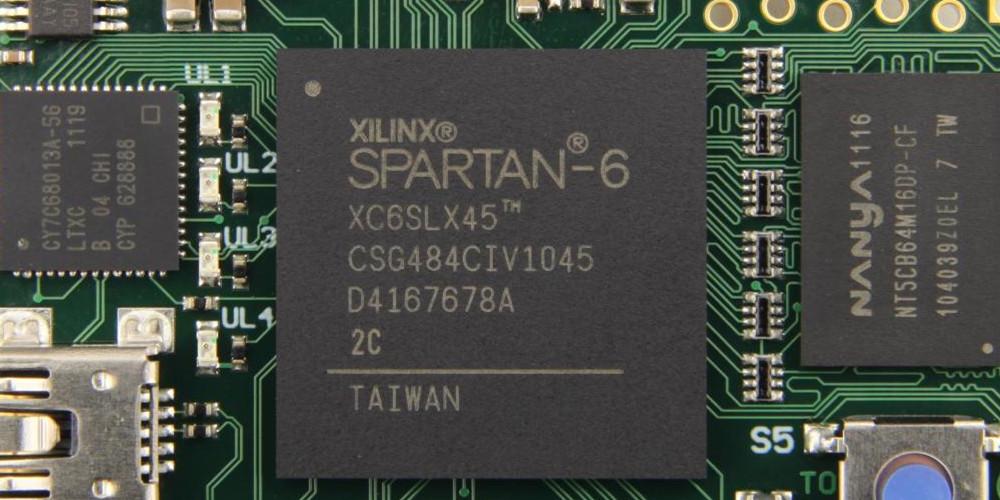
Spartan 6 family of FPGA devices offers great system integration capabilities for high-volume applications. This family offers more densities that range from 3,840 to 147,443 logic cells. Also, the Xilinx Spartan 6 offers faster and improved connectivity. Xilinx Spartan 6 is specifically built on a developed 45nm low-power copper process technology. This technology offers optimal balance of power, cost, and performance.
Xilinx Spartan 6 FPGA development board provides an improved dual-register 6-input look-up table (LUT) logic and a selection of built-in system-level blocks. The Spartan-6 FPGAs provide a low-cost programmable option to custom ASIC products. Also, Xilinx Spartan 6 provides the best solution for consumer-oriented DSP designs and high-volume logic designs.
Also, this FPGA is the programmable silicon basics for Targeted Design Platform that offers integrated hardware and software. These allow designers to target innovation as soon as their development cycle starts. Xilinx Spartan 6 FPGA offers technical support to cost-sensitive embedded applications. These cost optimized FPGAs feature embedded processors.
Spartan 6 FPGAs are next gen solutions to high-performance applications and cost-sensitive applications. Also, this best fit device family is widely used in other countries. Xilinx Spartan 6 includes a camera module and other advanced features.
What are the Features of Xilinx Spartan 6?
Xilinx Spartan 6 FPGA development board offers a lot of advanced features. Therefore, this FPGA has been able to provide the perfect solutions for some cost-sensitive and high-volume applications.
Low static and dynamic power
Xilinx Spartan 6 offers 45nm process technology for cost and low power. Also, this FOGA has a Suspend mode that maintains configuration with multi-pin wake-up. The low-power 1.0V core voltage and high performance 1.2V core voltage help to ensure low static and dynamic power.
Enhanced security
The enhanced security of this FPGA ensures design protection. Also, this FPGA comes with a Device DNA identifier for design authentication. There is an AES bitstream encryption in the bigger devices.
Clock management tike for enhanced performance
The clock management tile (CMT) improves the performance of Spartan 6 FPGA. This FPGA includes Digital Clock Managers (DCMs) get rid of duty cycle distortion and clock skew. Also, there is a frequency synthesis with phase shifting, simultaneous multiplication, and division.
Designed for low cost
Spartan 6 FPGA features several efficient integrated blocks and optimized selection of I/O standards. Also, these features offer a solution for high performance applications.
Simplified configuration
Xilinx Spartan 6 comes with a simplified configuration which provides support for low-cost standards. Also, this FPGA comes with a Multiboot that supports remote upgrade with several bitstreams. The DSP performance enables simplified configuration in Spartan 6 FPGA development board.
Configuration of Spartan 6 FPGA
Spartan-6 FPGA saves the configuration data in SRAM internal latches. Also, the number of configuration bits ranges between 3 Mb and 33 Mb. However, this depends on the user-design implementation options and the device size.
The configuration storage has to be reloaded anytime you power the FPGA. Also, you can pull the PROGRAM_B pin Low to reload this storage anytime. There are several data formats and methods for loading configuration.
When the FPGA produces the Configuration clock (CCLK) signal, the bit-serial configuration can be in master serial mode. The master SelectMAP mode delivers the CCLK signal during byte-wide configurations. Also, the slave SelectMAP mode accepts the CCLK signal for the 8 and 16 bite-wide transfer.
The ISE software utilizes a program known as BitGen to generate the bitsream configuration data. Therefore, the configuration process implements the following sequence:
- Clears the entire configuration memory
- Loads the configuration information commencing with the bus-width detection pattern.
- Detects Low power-up
- Checks the mode pins to determine if the configuration mode is slave or master or bit-serial or parallel.
- Begins a user-defined sequence of events like waiting for the PLLS or DCMs to lock and releasing the internal preset or reset of flip-flops.
The two common methods of configuring Spartan 6 FPGA are the Master Byte-wide Peripheral Interface (BPI) and Master Serial Peripheral Interface (SPI). Spartan 6 can configure itself through the BPI when linked to a parallel NOR flash. Also, the BPI isn’t available when utilizing Spartan 6 in CPG196 and TQG144 packages.
Xilinx Spartan 6 FPGA supports MultiBoot configuration. A MultiBoot Configuration allows the storage of two or more configuration bitstreams in a single configuration source. Also, the FPGA application regulates when to load a configuration.
Configurable Logic Block of Xilinx Spartan 6 FPGA

Spartan 6 features several configurable logic blocks (CLBs). Each CLB comprises two slices arranged side-by-side as part of two columns. The CLB slices in Spartan 6 are available in three types. These are SLICEX, SLICEM, and SLICEL. Also, each slice includes four Look-Up Tables (LUTs) miscellaneous logic, and eight flip-flops. The LUTS allow general-purpose combinatorial support.
SLICEX
Half of the slices in Spartan 6 FPGA are SLICEXs.
SLICEM
25 percent of slices in Spartan 6 are SLICEMs. You can configure each of the SLICEM LUTS as a dual 5-input LUTs or as a 6-input LUT with an output. Also, these LUTs can serve as distributed 64-bit RAM with two times 32 bits per LUT or as a two 16-bit shift registers (SRL 16s). You can register each LUT in a flip-flop within the configuration logic block.
SLICE L
25 percent of slices in Spartan 6 FPGA are SLICELs. SLICEL comprises all the features of SLICEM. However, it doesn’t have a shift register function.
Clock Management of Spartan 6
Spartan 6 FPGA development board features about six clock management tiles (CMTs). Each CMTs feature one PLL and two DCMs.
DCM
The DCM offers four phases of the input frequency. Also, it offers a dual frequency CLK2X and CLK2X180. Furthermore, the CLKDV output offers a fractional clock frequency you can phase-align to CLK0. The DCM executes the following functions:
- Phase shifting
You can shift all nine CLK outputs by a common amount. Also, configuration can help to establish a fixed DCM delay value. Also, the delay value can be dynamically decremented and incremented.
- Frequency synthesis
You can program the frequency synthesis outputs CLKFX180 and CLKFX to produce any output frequency.
- Spread-spectrum clocking
DCM can track and accept typical spread-spectrum clock inputs. Also, Spartan 6 FPGA development board can produce a spread-spectrum clock source from a fixed-frequency oscillator
PLL
The PLL can function as a frequency synthesizer for various frequencies. Also, it can function as a jitter filter for incoming clocks alongside the DCMs. The voltage-controlled oscillator (VCO) is the heart of the PLL. The VCO has a frequency range between 400 MHz and 1,080 MHz. Therefore, it spans more than one octave.
The pre-divider minimizes the input frequency and takes one input of the traditional PLL phase comparator. Also, the feedback divider serves as a multiplier since it divides the VCO output frequency before it feeds the other input of the phase comparator.
Clock Distribution
Spartan 6 FPGA features abundant clock lines that address the various clocking requirements of low skew, propagation delay, and high fanout.
- I/O clocks
I/O clocks serve the localized input and output delay circuits.
- Global clock lines
There are 16 global-clock lines in each Spartan 6 FPGA.
Block RAM
The dual-port block RAMs in every Spartan 6 FPGA ranges between 12 and 268. Each of these block RAMs store 18Kb. Also, each block RAM features two independent ports.
Synchronous operation
The clock controls each memory access. Also, it is possible to register all write enables, data address, and clock enables. An optional output data pipeline register enables higher clock rates at the expense of an extra cycle of latency.
The Input/Output of Xilinx Spartan 6
In Xilinx Spartan 6 FPGA, the number of input/output pins varies from 102 to 576. However, this depends on package size and device size. It is possible to configure every I/O pin. Also, you can comply these pins with a large number of standards using about 3.3V. The user manual for Xilinx Spartan 6 SelectIO describes the input/output compatibilities of the different I/O options. All package pins feature similar I/O capabilities asides from a few dedicated configuration pins and supply pins. Also, all user I/O pins are bidirectional. This means there no input-only pins.
Furthermore, all I/O pins are available in banks. There are six banks on the larger devices while four banks are on the smaller devices. Also, each bank features common Vcco output supply-voltage pins. This powers some input buffers. Furthermore, some single-ended inputs need VREF (externally applied voltage).
There are various dual-purpose pins in every bank. You must connect every VREF I/O pins to the same voltage rail when I/O standard needs a VREF voltage.
I/O electrical characteristics
It is important to know that single-ended outputs make use of a conventional CMOS push/pull structure. There are several I/O features available system designers to invoke in every I/O in their designs. You can configure all inputs and outputs as registered or combinatorial.
Spartan 6 FPGA Devices
XC6SLX75T-3FG676C XC6SLX150-2FG900C XC6SLX16-N3FTG256C
XC6SLX150T-N3FG676I XC6SLX4-2CPG196I XC6SLX150T-2FG900I
XC6SLX150-3FG900I XC6SLX9-FTG256BIV XC6SLX25-3FGG484C
XC6SLX16-3CPG196I XC6SLX75T-2FGG676I XC6SLX150-2CSG484C
XC6SLX75-2CSG484I XC6SLX9-3TQG144I XC6SLX9-L1TQG144I
XC6SLX9-3TQG144C XC6SLX9-3FTG256I XC6SLX9-3FTG256C
XC6SLX9-2TQG144I XC6SLX9-2FTG256I XC6SLX9-2TQG144C
XC6SLX9-2FTG256C XC6SLX9-2CSG225C XC6SLX9-2CSG225I
XC6SLX75T-2FGG484I XC6SLX75-3FGG484C XC6SLX75-3FGG484I
XC6SLX75-2FGG676I XC6SLX75-2FGG484C XC6SLX75-2FGG676C
XC6SLX75-2CSG484C XC6SLX45T-3FGG484C XC6SLX45T-3FGG484I
XC6SLX45T-2FGG484C XC6SLX45-3FGG676C XC6SLX45-3FGG676I
XC6SLX45-3FGG484I XC6SLX45-3CSG324C XC6SLX45-3CSG324I
XC6SLX45-2FGG484C XC6SLX45-2CSG484I XC6SLX45-2FGG484I
XC6SLX45-2CSG484C XC6SLX45-2CSG324I XC6SLX45-2CSG324C
XC6SLX25-3FTG256C XC6SLX25-3CSG324C XC6SLX25-3FGG484I
XC6SLX25-2FTG256I XC6SLX25-2CSG324I XC6SLX25-2FGG484C
XC6SLX16-3FTG256I XC6SLX16-3CSG324I XC6SLX25-2CSG324C
XC6SLX16-2FTG256C XC6SLX16-2CSG324I XC6SLX16-2CSG225I
XC6SLX150T-3FGG676I XC6SLX150T-3FGG484I XC6SLX150T-3FGG900C
XC6SLX150T-3FG676I XC6SLX150T-2FGG900I XC6SLX150T-2FGG484I
XC6SLX150-3FG676I XC6SLX150-3CSG484I XC6SLX150-3FGG676C
XC6SLX150-2FGG484I XC6SLX150-2FGG484C XC6SLX150-2FGG676I
XC6SLX150-2CSG484I XC6SLX100-3FGG676I XC6SLX100T-3FGG484I
XC6SLX100-3FGG484C XC6SLX100-2FGG484C XC6SLX100-3FGG484I
XC6SLX9-3CSG324C
Conclusion
Xilinx Spartan 6 FPGA development board provides enhanced system integration capabilities for high-volume applications. Also, this FPGA development features some basic elements that contribute to its performances when used in applications. The density and data rates of this FPGA development board are advanced.