Introduction
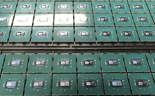
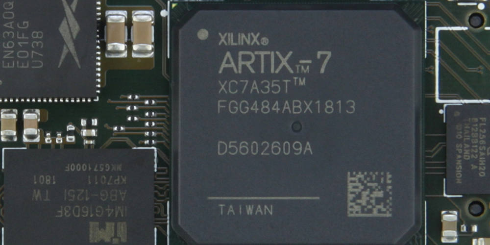
The Xilinx Artix-7 FPGA is a low-cost, low-power programmable logic device designed for high-volume applications. As part of the mid-range 7-Series FPGA fabric, Artix-7 provides an optimized combination of performance, power, and cost.
In this comprehensive guide, we will explore the architecture, capabilities, design tools and applications for the Artix-7 to understand its role within the Xilinx FPGA portfolio.
Artix-7 Family Overview
The Artix-7 family consists of seven major variants designed to address different market needs:
- Artix-7 FPGA – Balanced FPGA optimized for low-cost BOM.
- Artix-7 DSP FPGA – Cost-optimized DSP and math-intensive designs.
- Artix-7 A35T FPGA – Automotive reliability and qualification.
- Artix-7 100T FPGA – Optimized for low-power envelope tracking systems.
- Artix-7 XC12T FPGA – Extended temp -40C to +100C operation.
- Artix-7 HPC FPGA – High-performance computing FPGA.
- Artix-7 HT FPGA – High temp FPGA for up to 125°C.
The Artix-7 FPGA is the highest volume and most general purpose device. Within each family, there are multiple package and I/O combinations to choose from based on pin count and interfaces needed.
All Artix-7 devices utilize TSMC’s 28nm process and provide 1.0V core voltage along with 2.5V and 3.3V I/O operation.
Artix-7 Architecture
The Artix-7 architecture focuses on providing optimal price/performance/watt for high-volume applications. Some of the key architectural aspects include:
- ** Configurable Logic Blocks (CLB)** – Basic building block containing LUTs, flip-flops and carry logic. Artix-7 provides up to 215,000 CLBs.
- DSP Slices – Dedicated DSP resources with 25×18 multipliers. Artix-7 has up to 600 DSP slices.
- Block RAM (BRAM) – 36 Kb on-chip memory blocks. Up to 4.9 Mb BRAM in Artix-7.
- Mixed-Mode Clock Manager (MMCM) – Digital frequency synthesizers and clock management. Artix-7 includes up to 6 MMCMs.
- Transceivers – Select devices have up to 12.5Gbps transceivers for serial connectivity.
- Low-power modes – Various low-power modes including suspend and sleep modes.
- PCI Express – Integrated Gen2 x4 blocks for PCIe interface.
- Integrated ARM CPU – Cortex-A9 dual core CPU with MPCore subsystem (select devices).
Compared to the high-end Virtex-7, Artix-7 offers less resources but much lower cost and power suitable for mainstream applications.
Artix-7 FPGA Features
Let’s dive deeper into some of the key features of the Artix-7 architecture:
Configurable Logic Blocks
The CLBs provide the fundamental programmable logic resources. Each CLB includes:
- 2 slices with 4 total 6-input LUTs
- 8 flip-flops per slice
- Arithmetic carry logic
- Multiplexers and control logic
LUTs can implement any 6-input Boolean logic function. Flip-flops store results synchronously on the rising clock edge.
DSP Slices
DSP slices are dedicated DSP resources optimized for arithmetic. Each slice contains a fast 25×18 multiplier feeding into an adder/subtracter and optional accumulator register.
This enables high-performance arithmetic like FIR filters, FFTs, and complex math while minimizing overall logic utilization.
Block RAM
On-chip block RAM provides 36 Kb general purpose memory with two independent ports for access. Key capabilities:
- True dual-port operation
- Configurable aspect ratios from 16Kx1 to 512×72
- Optional ECC single error correction and detection
BRAM enhances memory bandwidth while reducing logic resource usage. Having sizable on-chip RAM is crucial for many applications.
Mixed-Mode Clock Manager (MMCM)
The MMCM components provide flexible clock manipulation and synthesis capabilities including:
- Clock frequency synthesis and phase alignment
- Low jitter clock generation and jitter filtering
- Zero-delay buffers
- Deskew and frequency stabilization feedback loops
This allows generating and distributing optimized clocks all parts of the FPGA design from a centralized clock source.
Transceivers
To provide multi-gigabit serialization, Artix-7 includes integrated transceivers capable of up to 12.5Gbps. Key features include:
- High-speed serial connectivity for protocols like PCIe, Ethernet, SATA etc.
- Multi-rate support from 155Mbps up to 12.5Gbps
- Deserializer and serializer for chip-to-chip links
- Sophisticated clocking options like clock data recovery (CDR)
Power Management
Artix-7 includes advanced power reduction capabilities:
- suspend mode reduces power to just 6mW static power
- sleep mode clock gating and power gating for unused sections
- FPGA logic can initiate low power modes via SUSPEND pins
- Lower core voltage of 1.0V Vs 1.2V for past devices
The power savings extend battery life critical for mobile and automotive applications.
Artix-7 Development Tools
Xilinx provides a complete tool flow for developing with the Artix-7 family:
Vivado Design Suite
Vivado offers system-level integration for IP-based designs:
- Create design using HDL, block diagrams, High-level synthesis
- Simulate behaviorally or post-implementation
- Full synthesis, place and route, timing closure
- Advanced analysis and optimization
- Generate FPGA bitstream
It enables the full development cycle from design through implementation for even the largest FPGAs.
SDx Development Environment
The SDx tools enable programming FPGAs at higher abstraction:
- C/C++ HLS conversion to RTL using Vivado HLS
- Libraries to efficiently access FPGA resources
- Debugging with breakpoints and variable watches
- Performance analysis and bottlenecks identification
- Compatible with OpenCL frameworks
This allows leveraging high-level languages and extending use model beyond just hardware designers.
Vitis AI
Built on SDx, Vitis AI enables machine learning on FPGAs:
- Run machine learning models built using frameworks like TensorFlow and Caffe
- Optimized machine learning runtime
- High-level graph optimizations
- Quantization and compression to optimize performance
Vitis AI accelerates deploying machine learning applications on FPGA platforms.
Artix-7 Applications
The Artix-7 value, lower power, and small form factor make it a fit for varied deployments:
Automotive/Avionics
Artix-7 A35T offers automotive grade qualification, reliability and extended temperature for engine control, driver assistance, infotainment etc.
Wireless Communications
The low cost and power make Artix-7 suitable for high volume baseband processing for 4G/LTE infrastructure. DSP performance accelerates modulation/demodulation algorithms.
Image Processing
Parallel pipelines enable real-time processing of video for surveillance, medical imaging, machine vision etc. Compression and filters can run efficiently via high bandwidth BRAM.
Video over IP
Quad 12.5Gbps transceivers allow implementing high density video over IP. Supports 4K UHD encoding, decoding and streaming.
Networking
For network switches, routers and packet inspection, Artix-7 enables high throughput data plane processing.
Military/Aerospace
Ruggedized Artix-7 XQ devices are available for extended temperature industrial and military systems. SEU mitigation enhances reliability and uptime.
Scientific Computing
For physics, genome sequencing, high-energy physics etc. the reconfigurable fabric accelerates parallel algorithms and floating point computations.
With its mix of resources and smaller size, Artix-7 serves high-volume mid-range application needs.
Conclusion
In summary, the Xilinx Artix-7 FPGA delivers an optimized combination of low cost, low power, and performance. With ample logic fabric, DSP slices, 36Kb BRAM blocks, 12.5Gbps transceivers, PCIe, memory controllers, ARM processors, and advanced power management, the Artix-7 architecture balances critical resources for mainstream FPGA applications. Paired with Xilinx’s mature Vivado and Vitis toolchains, the Artix-7 FPGA enables cost-sensitive yet highly capable programmable systems. For these reasons, Artix-7 continues to be a popular choice when low power consumption, small form factor, and total cost of ownership are critical design requirements.
Artix-7 FPGA FAQs
Here are some common questions about the Xilinx Artix-7 FPGA:
Q: What process node is the Artix-7 fabricated on?
A: Artix-7 FPGAs utilize TSMC’s 28nm HPL (High Performance, Low power) manufacturing process.
Q: What are the core voltage and I/O voltages for Artix-7?
A: The core voltage is 1.0V. I/O voltages are 2.5V and 3.3V for interfacing.
Q: What is the typical power consumption range of Artix-7 FPGAs?
A: Power consumption ranges from around 1 Watt for low-end devices up to 10 Watts for larger high-end Artix-7 FPGAs.
Q: Does the Artix-7 support partial reconfiguration?
A: Yes, the Vivado design tools do support dynamic partial reconfiguration to modify sections of the FPGA on the fly.
Q: What embedded processors can Artix-7 integrate?
A: Select Artix-7 devices offer hardened ARM Cortex-A9 dual core CPU subsystem for embedded processing.
Q: What is the main competitor FPGA to the Artix-7?
A: The primary competing FPGA is the Intel (Altera) Cyclone V series which also targets low cost, mid-range applications.
Q: What printed circuit board types are supported by Artix-7?
A: It supports mainstream low-cost laminate PCBs. Higher performance variants support advanced substrates.
Q: What are the typical BRAM and DSP slice counts for Artix-7 devices?
A: BRAM ranges from 1.9Mb to 4.9Mb. DSP slices range from 120 to 600. Counts vary by specific FPGA device.
Q: Does Artix-7 support SEU mitigation for soft errors?
A: Yes, the SEM IP core can be integrated to detect and correct single event upsets.
A COMPREHENSIVE PRODUCT OVERVIEW OF THE XILINX ARTIX 7 FPGA
More than 7,500 users worldwide build with Xilinx FPGAs because of the company’s dedication to cost-effective FPGA designs. About 50% of the company’s staff strength is dedicated software developers. Xilinx has yet to disappoint with the Artix 7 FPGA, another addition to the Xilinx series seven families.
The semiconductor giant announced the release of the Artix 7 FPGA in July 2012. Since the inclusion of this device, designers in the medical field, compact handheld radio, and various high-end applications have been leveraging its advantage.
We curated this article in a way that brings Artix 7 FPGA understanding to its simplest form. The report is for both long-time designers and newbies in FPGA design. This article will explain the following topics about the Xilinx Artix 7;
- Why Choose The Xilinx Artix 7.
- Suitable Applications For The Xilinx Artix 7
- Reviews From The Xilinx Artix 7 users.
- How To Decide Which FPGA Is Better For You.
- Xilinx Artix 7 AC701 FPGA Evaluation Kit
WHY CHOSE THE XILINX ARTIX 7
All Xilinx 7 series families come with 28nm optimum performance devices. Each of the seven series has certain specialized variations depending on the desired system performance. The Xilinx Artix 7 FPGAs have provided designers with a cost-optimized version in embedded memory, logic, LVDS I/O, signal processing, memory interfaces, and transceivers.
The Artix 7 comes with a MicroBlaze CPU which is highly configurable with a 32-bit RISC processor. In addition, this processor supports fast deployment and presets for microcontroller, real-time Processor, and application Processor use cases.
The Artix-7 FPGAs also allow other system integration capabilities, such as integrated advanced Analog Mixed Signal (AMS) technology. Since analog is the next level of integration, the Artix 7 accomplished this with an independent dual 12-bit, 1MSPS, 17-channel analog-to-digital converters in Artix-7 FPGAs. Additionally, The Artix 7 FPGA appeals to designers because of the following inclusive features;
- It enhanced programmable system integration.
- It provides A better scalable optimized architecture and transceiver line rates.
- There is Better system performance per watt with low-end wireless backhaul.
- It supports a better development platform designed around.
- It supports the Inclusion of AMS integration, high capacity FPGA, and DSP processing.
APPLICATIONS SUITABLE FOR XILINX ARTIX 7
The Artix 7 carries a Small form factor which breeds compact packaging and system flexibility. However, designers have found the Xilinx Artix 7 beneficial in the following applications:
- Multi-Protocol Machine Vision Cameras.
- Programmable Logic Controller
- Battery Powered Software Defined Radio
- 64-Channel Portable Ultrasound
- Wireless Backhaul: Point-to-Point 1024QAM Microwave Modem.
XILINX ARTIX 7 FEATURES
- Allows up to 200+ DMIPs MicroBlaze processor in Microcontroller, Real-Time Processor, or Application Processor configuration.
- It supports an Integrated memory interface for ease of access and power-sensitive applications.
- It helps a 50% total low power compared to the preceding generation
- Its Sub-watt performance ranges from 13K–to 2,000K logic cells
- It enhances 2xX logic, 2.5x block RAM, and 5.7x more DSP slices than Spartan 6 FPGAs.
- It possesses up to 6.6GBs transceivers enabling 211GBs peak bandwidth.
- Allows a Single and double differential I/O standards with speed support of up to 1.25GBs
- It supports up to 740 DSP48E1 slices with about 930 GMACs of signal processing.
- Possesses enhanced memory of 1,066Mb/s DDR3 memory, including SODIMMs support
- Provision of proven 28nm process, better speed grades, architecture, and quality.
- Supports enhanced Integrated IP blocks to mitigate development time and risk.
- It allows the use of Integrated wizards for rapid development of built-in blocks.
- Provides an enhanced environment for Bare metal, freeRTOS, and Linux support for MicroBlaze processor with drag n’ drop peripherals
- It supports development kits with IP and reference designs for quick design, starting with comprehensive tools.
- The Xilinx Artix 7 comes in a Low-cost, wire-bond, chip-scale BGA packaging.
- It Supports the lowest-power Industrial speed grade offering.
REVIEWS FROM THE XILINX ARTIX 7 USERS
Maybe you are still trying to determine what your team stands to benefit from building with the Xilinx Artix 7.
As a top industry player in the FPGA industry, the Xilinx Artix 7 has met the requirements of system design teams and individuals across various fields.
How did we know?
Here’s what some of our customers on the Amazon website have to say about their experiences building with the Xilinx Artix 7;
Sipy from the United States says:
Perfect lab FPGA board. Very powerful, lots of PMOD connectors, buttons, and switches, and can support a Microblaze/soft ARM CPU. Vivado Webpack Well supports it. There are a few examples for this board.
Brain Cannard also has this to say;
“Rock-solid, reliable, very well-documented, performant.”
MPE has this to say;
“I have been using these FPGA boards for some time now, and they have all worked great for me.
I recommend a 3D printed case to protect the components. Xilinx’s free version of their FPGA tools directly supports both versions of the board sold on Amazon. In addition, the board has an Arduino compatible expansion socket for easy prototyping. Finally, the Arty A7 has a 3D-printed protective case.
HOW TO DECIDE WHICH FPGA IS BETTER FOR YOU
One of the crucial decisions design teams make is selecting an FPGA package. Unfortunately, optimization problems always arise when deciding on the best FPGAs for their design. Also, problems come when the project requirements decide the trade-offs and compromises between features and capabilities.
Numerous FPGA features need consideration during the planning and decision stages of the system. Let us consider them briefly;
- FPGA PACKAGE
FPGA Package refers to how the FPGA pins arrangement is outside the FPGA. However, the PCB blueprint of the FPGA package presents a 2D rendition of the position where FPGA touches the PCB. Like conventional microcontrollers come in boxes like DIP, SOIC, QFP, etc. Similarly, FPGAs are available in different packages. Below is a list of FPGA prerequisites- Number of Multi-Gigabit Transceivers (MGT)
- The maximum speed of the I/Os and MGTs in an FPGA chip
- PCB routing rules, guidelines, and constraints
- Number of I/Os in an FPGA chip
Device Migration is also an important feature when selecting an FPGA. Device migration means that if you choose any FPGA with a particular package, you might have options available to upgrade to a higher-end FPGA within the same box. This feature provides a basis for leading system performance for cost-sensitive applications.
For example, in the Xilinx Artix-7 FPGA family, if you select XC7A50T, for instance, in an FGG484 package, you have five more Artix-7 devices with the same compatible footprint. It allows you to upgrade to a higher-end FPGA or downgrade to a lower-cost, lower-end FPGA and keep your hardware design the same. This feature provides mobility and flexibility in cost and optimal FPGA utilization.
- FPGA RESOURCES
Depending on the project type, designers can choose if the project requires many I/Os or just DSP slices. The significant FPGA resources you can choose from are;- MGT Transceivers
- Logic resources (LUTs, Flip-Flop, etc.)
- DSP slices
- Memory resources (Distributed RAM, Block RAM, etc.)
- Clock resources (PLL, MMCM, etc.)
- I/Os (Single-ended and differential)
- Hard-blocks such as ARM cores, PCIe, 100G Ethernet, Interlaken, etc
- INTERFACE
All FPGA communications require either via the general I/Os or transceivers. Hence, If the design needs a DisplayPort or PCI Express, choosing an FPGA with MGT transceivers is better. Also, if the design requires HDMI Input/Output, an FPGA that supports TMDS signaling should be used. - POWER CONSUMPTION
Power consumption, too, is another critical factor in picking an FPGA. It is one reason Xilinx rolled out the Artix 7 FPGA. Newer generations now use either 28nm or 14nm to cater to power requirements per logic cells. - COST
Undoubtedly, the cost is essential because it can heavily impact the design budget. Ordinarily, any additional FPGA feature attracts price; another reason to consider the Artix 7 is its cost-effectiveness.
XILINX ARTIX 7 FPGA AC701 EVALUATION KIT
An evaluation kit is a hardware environment that allows easy development and evaluation of the Artix 7 FPGAs.The Evaluation Kit provides a unique reference design to enable high-performance serial connectivity. It also supports advanced memory interfacing with a full license for the Northwest Logic DMA engine.
The Xilinx AC701 supports embedded processing features like;
- UART interfaces
- a 4-lane PCI Express interface,
- a tri-mode Ethernet PHY,
- general-purpose I/O,
- DDR3 SODIMM memory
- FPGA mezzanine card (FMC)
FEATURES OF THE ARTIX AC701 EVALUATION KIT
- Supports embedded processing with MicroBlaze, soft 32bit RISC
- Expand I/O with the FPGA Mezzanine Card (FMC) interface
- Develop networking applications with 10-100-1000 Mbps Ethernet (RGMII)
- Implement video display applications with HDMI out
- Demonstrates a high-performance data transfer system using a PCI Express® x4 Gen2
- Reference design implemented with Northwest Logic DMA engine attached to an AXI interface
- Advanced memory interface with 1GB DDR3 SODIMM up to 533MHz/1066Mbps
- Optimized for quickly prototyping cost-sensitive applications using Artix-7 FPGAs
- Hardware, design tools, IP, and pre-verified reference designs
CONCLUSION
The product reviews from customers give the credibility of the Artix 7 away. If you are a designer of high-end applications, then you don’t want to miss the Artix 7 FPGA.